Rank 6 of 7 in RP2350 dev board
GPT-6.1 Sol in Backplane
OpenAI's GPT-6.1 Sol on medium reasoning, in Backplane hub driving Codex CLI.
29.5 of 100−20 for a failed gate
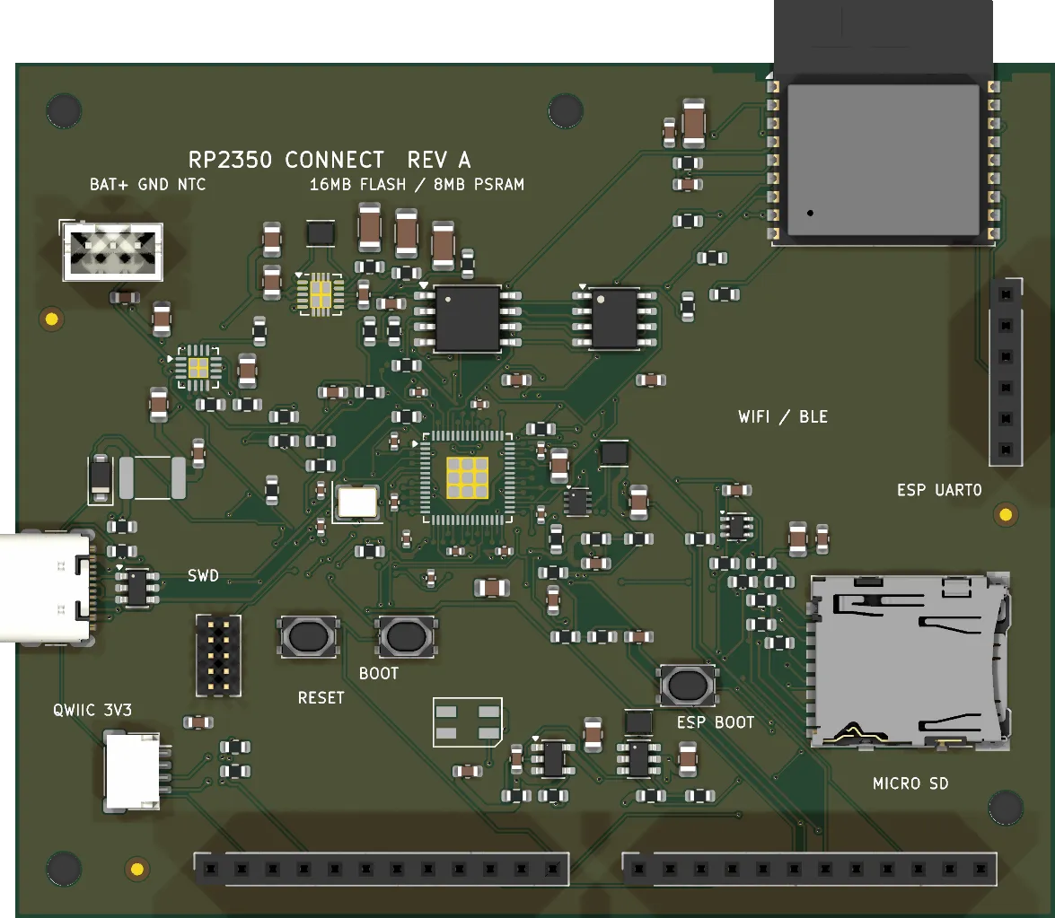
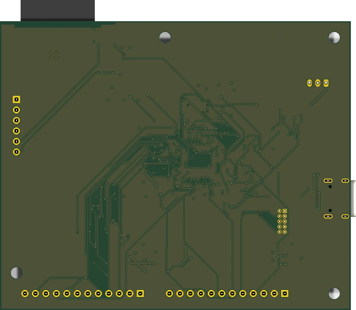
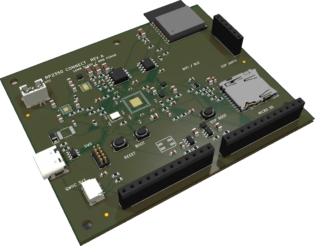
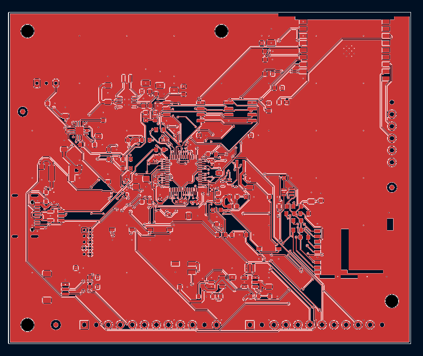
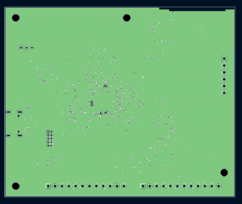
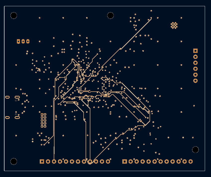
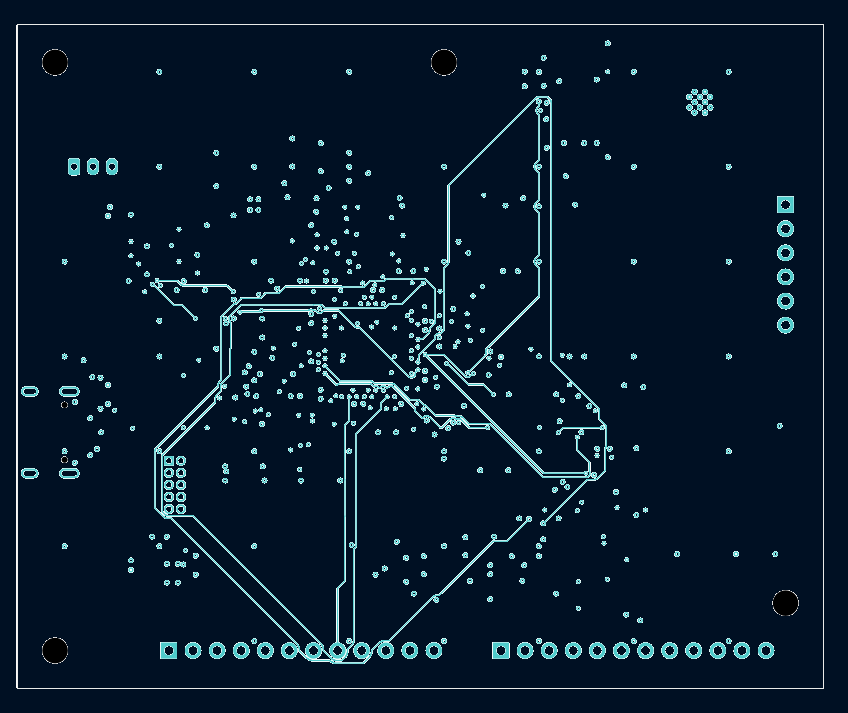
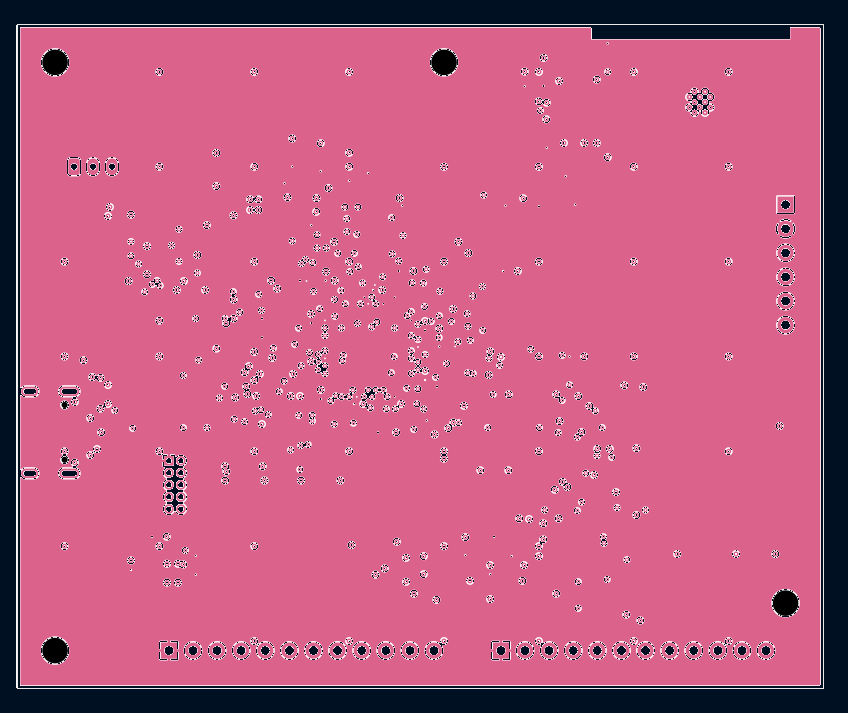
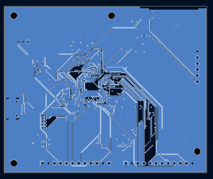
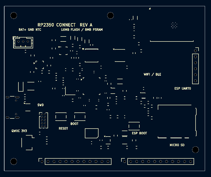
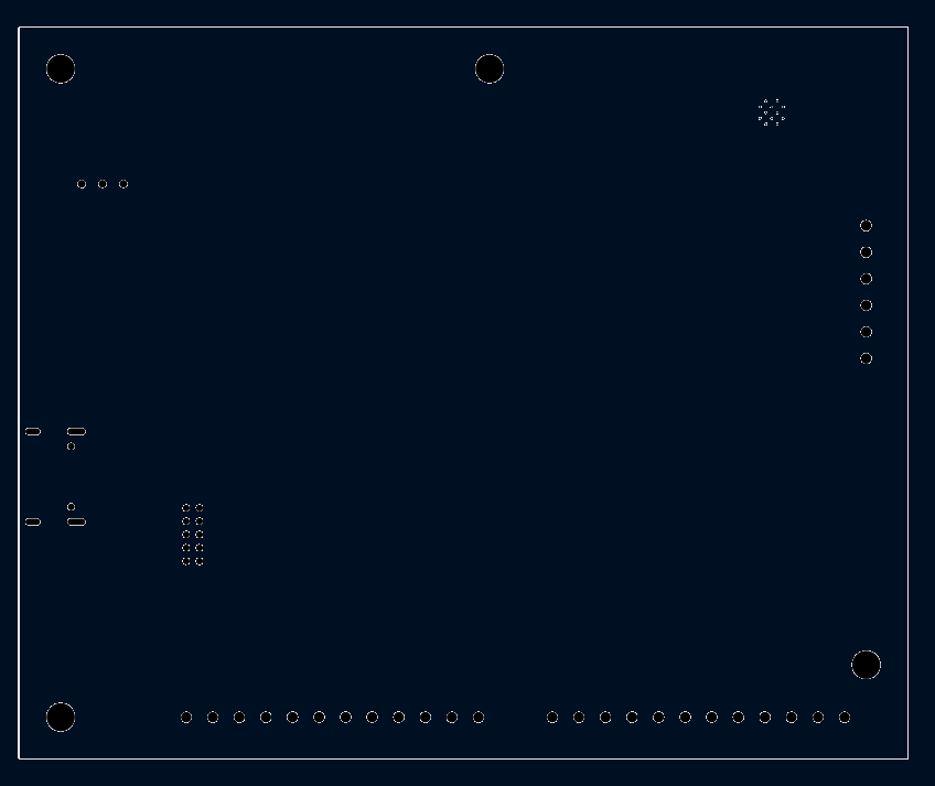
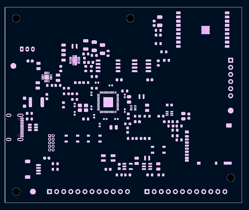
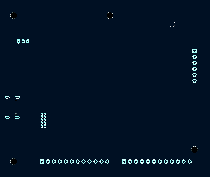
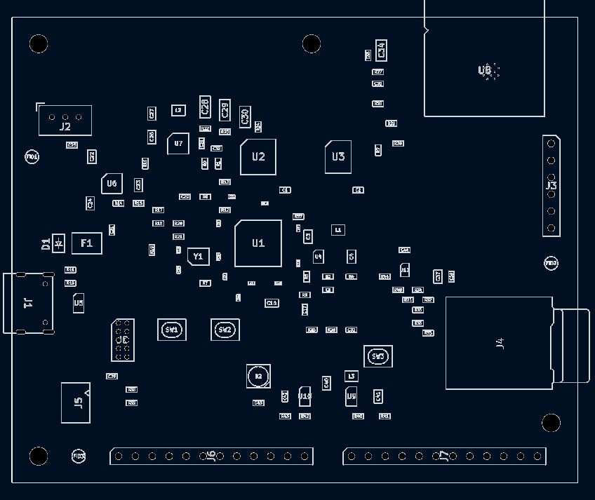
Rendered by kicad-cli with the run's own KiCad version. Dimensions in mm. The layers are the plots the AI judge saw, seen from the top, with their white background made dark. Click one to open it at full size.
- AI cost
- $5.81
- Time
- 1 h 38 min
- Tokens, incl. cache reads
- 28.6M
- 1 board
- $741.00
- 5 boards, per board
- $181.34
- Board size
- 85 × 70 mm
- Machine
- EC2 Ubuntu (c7i.2xlarge)
- backplane
- backplane-hub 0.15.0
- claudeCode
- 2.1.321 (Claude Code)
- codex
- codex-cli 0.167.0
- kicad
- 10.99.0-bp.4 (5dbc22d292704d02b609d5b7a0edc971f1b7f08b)
Score
Design review9 of 20
- Layout9 of 101 minus 0.1 per minor and 0.2 per major layout finding, down to 0
- Routing0 of 10the same, for routing findings
Circuit checks9.2 of 20
- Decoupling3.2 of 5RP2350 power pins with a capacitor within 3.2 mm
- USB protection5 of 50.5 for an ESD part on D+ and D−, plus 0.25 for each line with a series resistor
- Antenna keepout0 of 51 when there are keepouts and no copper is in them
- Battery drain1 of 51 at 5 µA or less drawn by unswitched battery dividers, falling linearly to 0 at 25 µA
Layout checks14.5 of 30
- Thermal pads2.7 of 10mean over the exposed pads of their vias over the number needed, 0 for a pad with no plane on another layer
- Grounding6.8 of 10USB, QSPI and microSD track length over a ground plane on the next layer
- Silkscreen5 of 5texts at least 0.8 mm high
- Board size0 of 51 at the Feather RP2350's 50.8 × 22.8 mm area or less, falling linearly to 0 at 5 times that area
Orderable12 of 20
- Fab notes5 of 51 when every fab option in the notes can be ordered from PCBWay
- Board5 of 51 when the board needs no rework
- BOM lines2 of 101 minus 0.2 for each BOM line that needs a fix, down to 0
Parts data4.8 of 10
- 3D models4.8 of 5parts with a 3D model
- Supplier part numbers0 of 5BOM lines with a valid number from at least one supplier
| The five groups | 49.5 |
|---|---|
| Failed gate: Fatal review finding | −20 |
| Score | 29.5 of 100 |
Gates
A board that fails a gate loses 20 points. The gates are the three checks below, every prompt feature, and any fatal review finding.
| Check | Result | What the check found |
|---|---|---|
| Crystal and load capacitors | Pass | Y1 ABM8-272-T3 (CL 10 pF) between XIN and XOUT via R7 1k; load caps /XIN: C18 15p; /XOUT: C19 15p; needs 10.5–17.5 pF per side for 3 pF stray |
| BOOTSEL and RUN buttons | Pass | QSPI_SS (/FLASH_CS) → R9 → SW2 → GND; RUN (/RUN) → SW1 → GND |
| Charger power path | Pass | U6 BQ24074RGTR: U6 IN (/VBUS) is on J1 VBUS; BAT (/VBAT) goes to J2; U7 TPS63060DSCR makes /3V3 from OUT (/VSYS) |
Prompt features
- Found RP2350 U1
- Found QSPI flash U2
- Found PSRAM U3
- Found USB-C J1
- Found Wi-Fi and BLE U8
- Found microSD J4
- Found Qwiic J5
- Found RGB LED D2
- Found Power-path charger U6
- Found Battery monitoring R25
Design review 9 of 20
Opus 5.5 reviewed an anonymous copy of the board and listed 11 findings. Layout and routing each start at 10 points.
Fatal
Other
The USB VBUS TVS diode is fitted backwards. The schematic uses a bidirectional TVS symbol, but SMF5.0A is a unidirectional part. Its cathode sits on GND and its anode on VBUS, so the diode is forward-biased across USB 5 V. With F1 downstream, it shorts the host's VBUS, and the board can't power from USB or the TVS burns.
Evidence
D1 (SOD-123F at 107.0, 134.0): pad 1 at (107.0, 135.4) is /GND and pad 2 at (107.0, 132.6) is /VBUS_RAW. The footprint marks pad 1 as the cathode with the silkscreen bracket at x=-2.21 and the F.Fab bar at x=-0.35. Littelfuse lists SMF5.0A as 'Uni-directional', with the cathode marked by the color band. Symbol connect:D_TVS is described as 'Bidirectional transient-voltage-suppression diode'.
Major
Routing
The charger output to the 3.3 V buck-boost is a 0.25 mm trace that passes through two 0.2 mm-drill vias, but it carries up to 1.5 A. The charger's OUT capacitor C23 hangs off a 0.15 mm trace.
Evidence
U6 pads 10/11 (116.44, 124.75/125.25) go out on F.Cu at 0.25 mm to via (117.061, 124.982), 0.45/0.2 mm. The path continues on B.Cu at 0.25 mm for 3.39 mm to via (117.061, 121.589), 0.45/0.2 mm. It then runs on F.Cu at 0.25 mm for 3.73 mm to (119.7, 118.95), and U7 pads 2/3 are fed by 0.25 mm F.Cu stubs at (122.3-123.24, 118.5-119.25). C23 pad 1 (119.0, 126.2) reaches VSYS through B.Cu at 0.15 mm, (119.0, 126.2)-(117.8, 125.0)-(117.05, 125.0).
The battery path from J2 to the charger's BAT pins narrows to 0.25 mm and passes through two 0.2 mm-drill vias, but it carries up to 1.5 A.
Evidence
J2 pad 1 (106.0, 115.0) runs on B.Cu at 0.5 mm to via (109.575, 120.2), then on F.Cu at 0.5 mm to (112.0, 121.95). From there it runs on F.Cu at 0.25 mm to via (112.0, 122.8925), 0.45/0.2 mm, and on B.Cu at 0.25 mm for 1.51 mm to via (112.0, 124.4005), 0.45/0.2 mm. The last leg is F.Cu at 0.25 mm, (112.62, 124.75)-(113.56, 124.75/125.25), into U6 pads 2/3.
The buck-boost inductor connections are 0.18 mm traces about 5 mm long, and they carry the full inductor current. The TPS63060 datasheet requires wide, short traces for the main current path and the inductor as close as possible. The board's average inductor current limit is 2.0 to 2.5 A.
Evidence
BB_L1 runs from U7 pad 1 (123.525, 118.0) to L2 pad 1 (124.275, 114.0), 5.23 mm on F.Cu at 0.18 mm through (122.79, 117.63). BB_L2 runs from U7 pad 10 (126.475, 118.0) to L2 pad 2 (125.725, 114.0), 5.23 mm on F.Cu at 0.18 mm through (127.21, 117.63). The TPS63060 datasheet covers this in section 11.1 Layout Guidelines, and the electrical characteristics give ISW average inductance current limit = 2000/2250/2500 mA.
The 3.3 V regulator output, which supplies the whole board including ESP32-C3 Wi-Fi bursts, leaves U7 through one 0.15 mm trace and a single via to the In4 plane. The output capacitors reach VOUT only through that via and the plane.
Evidence
U7 pad 9 VOUT (126.475-126.76, 118.5) is the only copper on F.Cu. It runs at 0.15 mm, (126.76, 118.5)-(127.05, 118.5)-(128.175, 117.375)-(128.175, 116.75), to one via (128.175, 116.75), 0.55/0.25 mm, into the In4.Cu 3V3 pour. C28/C29/C30 pad 1 connect only through their own vias at (129.0, 114.975), (132.0, 115.475) and (135.0, 116.475).
The microSD clock detours around the board. GPIO10 runs about 100 mm down to the bottom edge and back up to series resistor R37 at U1's opposite corner, then 34 mm more to J4. With 5 vias, the 33 ohm resistor sits 100 mm from its driver, so it no longer damps the clock edges.
Evidence
SD_CLK_DRV goes from U1 pad 14 (133.55, 136.4) to via (131.75, 136.4), then 5.2 mm on B.Cu to via (129.7, 141.2). It continues 92.3 mm on In2.Cu at 0.127 mm, with a bounding box (129.7-161.6, 130.3-167.05), to via (141.55, 130.275) and R37 pad 1 (142.175, 130.0). That's 100.1 mm against 10.7 mm straight. SD_CLK goes from R37 pad 2 to via (145.97, 130.0), 29.3 mm on B.Cu to via (163.13, 149.305), then to J4 pad 5 (165.275, 150.625), 34.2 mm.
The microSD data lines cross the whole board with up to 5 vias each. The SPI pins GPIO8-11 are on U1's west side, and J4 is at the east edge.
Evidence
U1 pad 13 to J4 pad 2 (SD_CS) is 62.2 mm with 5 vias, against 33.7 mm straight. U1 pad 15 to J4 pad 3 (SD_MOSI) is 44.4 mm with 5 vias, including vias (132.45, 136.8), (149.6, 142.5), (155.05, 142.5), (157.025, 143.025) and (161.675, 142.5), mostly on In3.Cu. U1 pad 12 to J4 pad 7 (SD_MISO) is 48.9 mm with 2 vias, mostly on In2.Cu. U1 pads 12-15 are at x=133.55, and J4 pins are at x=165.275.
The PSRAM chip select detours around the flash and PSRAM and changes layer 6 times. It is three times longer than the direct path.
Evidence
U1 pad 2 (133.55, 131.6) to U3 pad 1 (146.525, 119.095) is 56.8 mm against 18.0 mm straight. It uses 6 vias at (129.672, 132.016), (131.611, 122.182), (131.611, 123.567), (132.58, 123.567), (135.074, 126.06) and (138.536, 126.614). On F.Cu it loops down to (147.5, 130) and around U3's east side to (154, 121) before reaching pin 1 and R2.
Minor
Layout
The PSRAM sits past the flash, about 13 mm from the RP2350 QSPI pins, so its QSPI branches are 22 to 29 mm long.
Evidence
U3 pad 4 (146.525, 122.905) is 12.8 mm from U1 pad 55 (136.2, 130.55), and U3 pad 6 (151.475, 121.635) is 18.0 mm from U1 pad 56. U1 to U3 path lengths are CLK 24.8 mm, D0 22.1 mm, D1 26.9 mm, D2 25.7 mm and D3 29.4 mm.
Routing
Several QSPI lines change layers even though flash and PSRAM sit on the same side as U1. QSPI_D1 has 4 vias, and QSPI_CLK, QSPI_D3 and FLASH_CS have 2 each.
Evidence
QSPI_D1 vias are at (134.758, 120.47), (134.758, 121.856), (136.42, 127.257) and (134.6, 129.45). QSPI_CLK vias are at (137.925, 131.375) and (140.675, 122.25). QSPI_D3 vias are at (136.2, 129.45) and (139.48, 120.365), and its U1 to U2 path is 17.4 mm against 11.1 mm straight. FLASH_CS vias are at (129.0, 122.825) and (129.975, 125.2).
The USB pair is routed apart. D- stays on F.Cu, but D+ drops to In2 and detours under the crystal to a series resistor 4 mm away from D-'s. D+ ends up 13 mm longer than D- with 4 vias against D-'s 2.
Evidence
J1 pad A6 to R13 pad 1 (USB_DP) is 40.4 mm. It runs on F.Cu at 0.22 mm to via (124.2725, 138.955), then 17.5 mm on In2.Cu at 0.127 mm across Y1 (124.3-131.2, 125.1-139.0) to via (131.175, 125.125). R13 pad 2 to U1 pad 52 is 16.0 mm through vias (135.96, 125.55) and (137.4, 128.75). J1 pad A7 to R12 pad 1 (USB_DM) is 36.0 mm on F.Cu at 0.22 mm, and R12 pad 2 to U1 pad 51 is 6.7 mm. R13 is at y=124.8 and R12 at y=129.0.
Opus 5.5's notes
I finished the review and saved it to review.json. The file is valid JSON and has 11 findings. When I checked it a final time, I found that 5 of the 16 findings I had before broke your exclusion rules, so I removed them.
| Area | Severity | Finding |
|---|---|---|
| other | fatal | D1: the SMF5.0A TVS diode is backwards across USB VBUS. It conducts across the 5 V input, so the board either can't power from USB or the TVS burns out. |
| routing | major | VSYS from the charger to the buck-boost is a 0.25 mm trace through two 0.2 mm vias, but it carries up to 1.5 A. |
| routing | major | The VBAT path from J2 to the charger narrows to 0.25 mm. |
| routing | major | The traces to the buck-boost inductor (BB_L1/BB_L2) are 0.18 mm wide and about 5 mm long. |
| routing | major | The 3.3 V output feeds the whole board, including the ESP32 Wi-Fi bursts, through a 0.15 mm trace and a single via. |
| routing | major | SD_CLK detours around the board, about 134 mm long. |
| routing | major | The SD data lines cross the whole board with up to 5 vias each. |
| routing | major | PSRAM_CS detours and changes layer 6 times. |
| routing | minor | Several QSPI lines have extra layer changes. |
| routing | minor | USB D+ drops to In2 and detours under the crystal. It ends up 13 mm longer than D-. |
| layout | minor | The PSRAM sits about 13 mm from the QSPI pins, so its branches are 22 to 29 mm long. |
What I removed
- Crystal routing, crystal placement and the XOUT_DRV stub: your list says automated checks cover the crystal circuit, and I couldn't confirm any of these would stop the oscillator.
- Buttons in the board interior: BOOTSEL/RUN buttons are on the list too.
- SD_CS stub: it's one of KiCad's two DRC warnings, and DRC is excluded. The XOUT_DRV stub is the other one.
- USB, downgraded from major to minor: I took out the claim that the pair is uncoupled because that's about impedance, which is excluded. RP2350 USB runs at full speed (12 Mbps), so a 13 mm length mismatch has almost no electrical effect. That leaves a messy detour with extra vias.
Upgrade
The schematic and board were upgraded in place to the connector's KiCad version. The only file changes are the version lines and one removed (embedded_fonts no) line. KiCad also created board.kicad_prl.
I didn't run /cleanup, as you asked. No subagents were used.
Circuit checks 9.2 of 20
Decoupling
3.2 of 59 of 14 RP2350 power pins have a capacitor within 3.2 mm.
| Pin | Pad | Net | Nearest capacitor | Distance |
|---|---|---|---|---|
| IOVDD | 1 | /3V3 | C6 | 2.57 mm |
| DVDD | 6 | /1V1 | C15 | 3.45 mm |
| IOVDD | 11 | /3V3 | C7 | 3.66 mm |
| IOVDD | 20 | /3V3 | C8 | 2.57 mm |
| DVDD | 23 | /1V1 | C13 | 3.59 mm |
| IOVDD | 30 | /3V3 | C10 | 3.2 mm |
| IOVDD | 38 | /3V3 | C9 | 3.1 mm |
| DVDD | 39 | /1V1 | C13 | 6.4 mm |
| ADC_AVDD | 44 | /ADC_3V3 | C17 | 12.15 mm |
| IOVDD | 45 | /3V3 | C9 | 2.55 mm |
| VREG_AVDD | 46 | /3V3 | C12 | 2.87 mm |
| VREG_VIN | 49 | /3V3 | C12 | 2.55 mm |
| USB_OTP_VDD | 53 | /3V3 | C12 | 2.6 mm |
| QSPI_IOVDD | 54 | /3V3 | C12 | 2.71 mm |
USB protection
5 of 5- ESD parts on D+ and D−
- U5
- D+ nets, connector to RP2350
- /USB_DP → /USB_DP_MCU series resistor
- D− nets, connector to RP2350
- /USB_DM → /USB_DM_MCU series resistor
Differential pair, not scored
- D+ and D− length
- 58.54 mm and 42.65 mm
- Mismatch
- 15.89 mm
- Vias
- 6
- Longest coupled stretch
- 9.93 mm on F.Cu, 0.22 mm wide, 1.68 mm gap
- Differential impedance
- no stackup
Antenna keepout
0 of 52 keepouts cover the Wi-Fi module U8.
| Keepout | Layers | Copper inside |
|---|---|---|
| U8 footprint | F.Cu, B.Cu, In1.Cu, In2.Cu | fill /3V3 on In4.Cu |
| Board, ESP32 antenna no copper | F.Cu, B.Cu, In1.Cu, In2.Cu, In3.Cu, In4.Cu | none |
Battery drain
1 of 5Unswitched dividers draw 21 µA from a full battery, even when the board is off.
| Divider | Buffered by | Switched by | At 4.2 V |
|---|---|---|---|
| R25 100k / R26 100k | none | none | 21 µA |
Layout checks 14.5 of 30
Thermal pads
2.7 of 10| Exposed pad | Net | Vias | Needed | Plane on another layer |
|---|---|---|---|---|
| U1 | /GND | 0 | 9 | yes |
| U6 | /GND | 0 | 5 | yes |
| U7 | /GND | 4 | 5 | yes |
Grounding
6.8 of 10| Bus | Over ground | Track length | Share |
|---|---|---|---|
| USB | 85.5 mm | 101.2 mm | 84.5% |
| QSPI | 134.3 mm | 154.8 mm | 86.8% |
| microSD | 216.3 mm | 383.3 mm | 56.4% |
| All three | 436.1 mm | 639.3 mm | 68.2% |
Silkscreen
5 of 50 of 11 texts are below PCBWay's 0.8 mm minimum. The smallest is 0.85 mm.
Board size
0 of 585 × 70 mm, 5950 mm². The Feather RP2350 is 50.8 × 22.8 mm.
Orderable 12 of 20
| 1 board | 5 boards | |
|---|---|---|
| PCBs | $593.00 | $593.00 |
| Assembly | $88.00 | $115.12 |
| Components | $60.00 | $198.57 |
| Total | $741.00 | $906.69 |
| Per board | $741.00 | $181.34 |
PCBWay's instant quote for the options in the fab notes, without shipping. PCBWay makes at least 5 PCBs, so 1 board is 5 PCBs with 1 assembled. Parts are at distributor list prices. The prices include the fixes below.
Fixes made to price the order
| Area | Parts | Problem | Fix |
|---|---|---|---|
| BOM | R3 | Invalid MPN: 83.5k is not an E96 value, so Yageo's 1% RC series doesn't make it | Priced KOA RN73R1JTTD8352B25, an 83.5k 0.1% 0603 |
Fab notes
5 of 5No fixes needed.
Board
5 of 5No fixes needed.
BOM lines
2 of 104 of 54 BOM lines need a fix.
- R3: Invalid MPN: 83.5k is not an E96 value, so Yageo's 1% RC series doesn't make it
- not stocked for 5 boards: C3 C16 C40; C17 C21; C28 C29 C30 C34
Parts data 4.8 of 10
3D models
4.8 of 55 parts have no 3D model the run's KiCad can load: D2, F1, U1, U6, U7.
Supplier part numbers
0 of 50 of 54 BOM lines have a valid supplier part number.
LCSC 0%, Digi-Key 0%, Mouser 0%
Stock
92.6% of 54 BOM lines are stocked for 5 boards at LCSC, JLCPCB or Digi-Key.
| Parts | MPN | Needed |
|---|---|---|
| C3 C16 C40 | GRM21BR61A475KA73L | 15 |
| R3 | RC0603FR-0783K5L | 5 |
| C17 C21 | GRM188R61C105KA93D | 10 |
| C28 C29 C30 C34 | GRM31CR61A226KE19L | 20 |
| Parts | MPN | At |
|---|---|---|
| C1 C2 C20 C25 C31 C33 C35 C36 C38 C39 C42 C43 C44 | GRM188R71C104KA01D | Digi-Key |
| C3 C16 C40 | GRM21BR61A475KA73L | Digi-Key |
| C4 C22 C23 C24 C26 C27 C37 C41 | GRM21BR61A106KE19L | Digi-Key |
| C17 C21 | GRM188R61C105KA93D | LCSC, Digi-Key |
| C28 C29 C30 C34 | GRM31CR61A226KE19L | LCSC, Digi-Key |
DRC and ERC
| Errors | Warnings | Unconnected | |
|---|---|---|---|
| DRC | 0 | 2 | 0 |
| ERC | 0 | 0 |
DRC by type: track_dangling 1, via_dangling 1.
Files
The agent's README
RP2350 Connect — revision A
An 85 × 70 mm RP2350A development board designed for PCBWay turnkey PCB fabrication and assembly. All 118 electrical components are fitted, including the connectors and sockets. PCBWay procures every BOM item; there are no customer-supplied parts or DNP options. A protected LiPo battery, microSD card, USB cable, and debugger are external accessories.
Open boards/rp2350-connect/rp2350-connect.kicad_pro. Its schematic, board, and local symbol/footprint libraries form the canonical project. .backplane.json points to it. Manufacturing outputs are in fab/; scripts and intermediate verification files are in scripts/ and build/.
Hardware
| Function | Implementation |
|---|---|
| Processor | Raspberry Pi RP2350A, QFN-60; A2 or newer silicon required |
| Program flash | Winbond W25Q128JVSIQ, 16 MB QSPI |
| Working memory | AP Memory APS6404L-3SQR-SN, 8 MB PSRAM; shared QSPI bus, independent CS on GPIO0 |
| USB | USB-C, USB 2.0 full-speed power/data; two 5.1 kΩ CC resistors, ESD protection, TVS, resettable fuse |
| Battery charging | TI BQ24074, USB/battery power path, nominal 499 mA charge current, pack thermistor input |
| Main rail | TPS63060 buck-boost, regulated 3.3 V from the charger system output |
| Core rail | TPS62823 external 1.101 V buck supply |
| Wireless | ESP32-C3-WROOM-02-N4, 2.4 GHz Wi-Fi and Bluetooth LE, RP2350 UART with RTS/CTS |
| Storage | Hirose microSD slot, SPI1, switched 3.3 V supply |
| I²C | JST SH Qwiic/STEMMA QT connector; 3.3 V, 4.7 kΩ pullups |
| RGB | SK6812MINI; separate 5 V boost and AHCT level buffer |
| Debug/expansion | Installed SWD header, separate ESP UART0 socket, two 12-pin GPIO sockets, reset and boot buttons |
| PCB | Six copper layers, 1.6 mm FR-4, ENIG; all components on top |
Design decisions and operating requirements
The ESP module provides both required radios without RP2350 RF circuitry. Its PCB antenna overhangs the north edge; keep the antenna area clear of copper, batteries, metal, and enclosure hardware. The final stack is F.Cu signal/GND pour, In1.Cu GND, In2.Cu signal, In3.Cu signal, In4.Cu 3V3, B.Cu signal/GND pour. The extra signal layers make room for the fine-pitch MCU escapes. Minimum copper spacing is 0.10 mm, minimum track width 0.127 mm, and routing vias are 0.45/0.20 mm. Filled and copper-capped vias are required, including vias under solder pads.
The RP2350 uses an external core regulator per the external-supply circuit in the RP2350 datasheet. VREG_FB is grounded and LX is intentionally unconnected. Firmware must set VREG.HIZ and must not attempt to change core voltage through the internal regulator. This also avoids the special polarity requirement of the RP2350 internal-regulator inductor. The core rail is fixed near 1.10 V; qualify any overclocking separately.
The battery connector is JST PH, three pins: 1 = battery positive, 2 = ground, 3 = 10 kΩ NTC thermistor. This is not the usual two-pin hobby battery connector. Use a protected single-cell 4.2 V lithium-ion/LiPo pack, at least 1000 mAh and rated for at least 500 mA charging, with an appropriate 10 kΩ NTC. The charger does not replace pack overcurrent/undervoltage protection. Do not connect two cells, LiFePO4, or a pack without its required thermistor. Verify mating-cable polarity before use. Battery voltage is 2 × ADC(GPIO26), using the measured ADC reference; the divider draws approximately 21 µA at 4.2 V.
At reset the charger input limit is 100 mA, ESP is held in reset, and microSD power is off. Firmware must enumerate USB and obtain its power budget before enabling the radio/card and increasing the input limit. BQ24074 EN1/EN2: 0/0 = 100 mA, 1/0 = 500 mA, 0/1 = resistor-programmed limit, 1/1 = input suspend. The resistor limit is approximately 500 mA; it is not USB-C current-advertisement detection. CE is active low: GPIO19 high disables charging. Dynamic power management gives the board load priority over charging. Respect USB suspend and unconfigured-device current limits. Standalone USB charger operation requires a firmware power policy; no USB-PD negotiation is provided. Keep RGB brightness low until the available power is known. External 3V3 loads share this budget; no maximum expansion current is guaranteed without thermal/load qualification.
Initialize SD bus outputs low or as inputs before GPIO1 enables its supply. Avoid driving unpowered card inputs high. Start at standard SD initialization speed, then qualify operation up to 24 MHz. Start QSPI PSRAM conservatively and validate timing before increasing its clock. The PSRAM CS uses GPIO0, which requires board-specific memory initialization rather than a generic Pico board configuration.
GPIO assignment
| GPIO | Use |
|---|---|
| 0 | PSRAM CS1 |
| 1 | SD power enable; also J6 pin 3 |
| 2 / 3 | I²C SDA / SCL |
| 4 / 5 | RP UART TX / RX to ESP GPIO6 RX / GPIO7 TX |
| 6 / 7 | RP CTS / RTS to ESP GPIO4 RTS / GPIO5 CTS |
| 8 / 9 / 10 / 11 | SD MISO / CS / clock / MOSI |
| 12–15 | Expansion GPIO |
| 16 / 17 | ESP enable / boot strap |
| 18 / 20 | Charger EN1 / EN2 |
| 19 | Charger disable (CE high) |
| 21 / 22 | Charger status / USB power-good, active low |
| 23 | RGB data, GRB at 800 kHz |
| 24 | microSD detect, active low |
| 25 | Expansion GPIO |
| 26 | Battery ADC; also exposed at J7 pin 6 |
| 27–29 | Analog-capable expansion GPIO |
Qwiic J5 pins: GND, 3V3, SDA, SCL. Expansion and debug pin-by-pin definitions are in fab/connector-pinout.csv and the schematic. Exposed status/control nets already have board functions: take care when driving them from external hardware. GPIOs are 3.3 V logic.
Programming and manufacture
The RP2350 ROM supports USB recovery: hold BOOT, press/release RESET, then release BOOT and load a board-specific UF2. SWD is available at J8. ESP UART0 is independently available at J3 for loading the official ESP32-C3-WROOM-02 ESP-AT firmware. Its command UART is GPIO6/7/5/4, not the UART0 programming pins. Use a 3.3 V UART adapter, share ground, and power the board through USB/battery rather than connecting an adapter supply. Drive ESP EN high and hold ESP BOOT low during reset to enter download mode; release BOOT afterward. For an empty RP2350, EN can be driven from the programming fixture because the MCU pin is initially high impedance. Match flashing offsets to the exact official firmware archive. Application firmware and radio firmware binaries are not included; this is a hardware design, and PCBWay should leave flash blank unless a subsequently approved binary is supplied.
fab/PCBWAY-INSTRUCTIONS.md specifies procurement, stackup, via treatment, assembly, orientation, and first-article checks. fab/TEST-PLAN.md describes hardware acceptance and the additional firmware-assisted tests needed to qualify the first article. Gerbers, separate plated/non-plated drill files, BOM, placement CSV, assembly drawings, schematic PDF, electrical netlist, and verification reports are included. The position file includes both SMT and through-hole components. PCBWay must check rotations against the assembly drawing and local footprints rather than assuming a distributor's rotation convention.
Review status
Verification results are recorded in fab/verification/ and fab/RELEASE-STATUS.md. This revision has not been physically built or measured. Firmware timing, RF performance, USB signal integrity, charger thermistor thresholds, thermal behavior, and battery operation require first-article validation. The schematic nets were independently compared to the frozen component specification. Hardware checks do not establish functional firmware correctness.
KiCad was authored with Backplane KiCad 10.99.0-bp.4. A compatibility export, when provided in fab/source-kicad10/, is accompanied by its conversion report; use the canonical source for edits. Backplane returned the canonical viewer path but did not confirm viewer refresh/history, so exported drawings serve as the static review evidence.
Manufacturer references: RP2350 datasheet, BQ24074, TPS63060, TPS62823, ESP32-C3-WROOM-02, and official ESP-AT hardware pinout.