Rank 5 of 7 in RP2350 dev board
GPT-6.1 Sol in Codex desktop + text-to-cad
OpenAI's GPT-6.1 Sol on medium reasoning, in Codex in the ChatGPT desktop app, with computer use and the text-to-cad plugin.
56.4 of 100
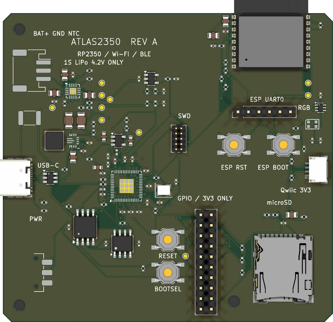
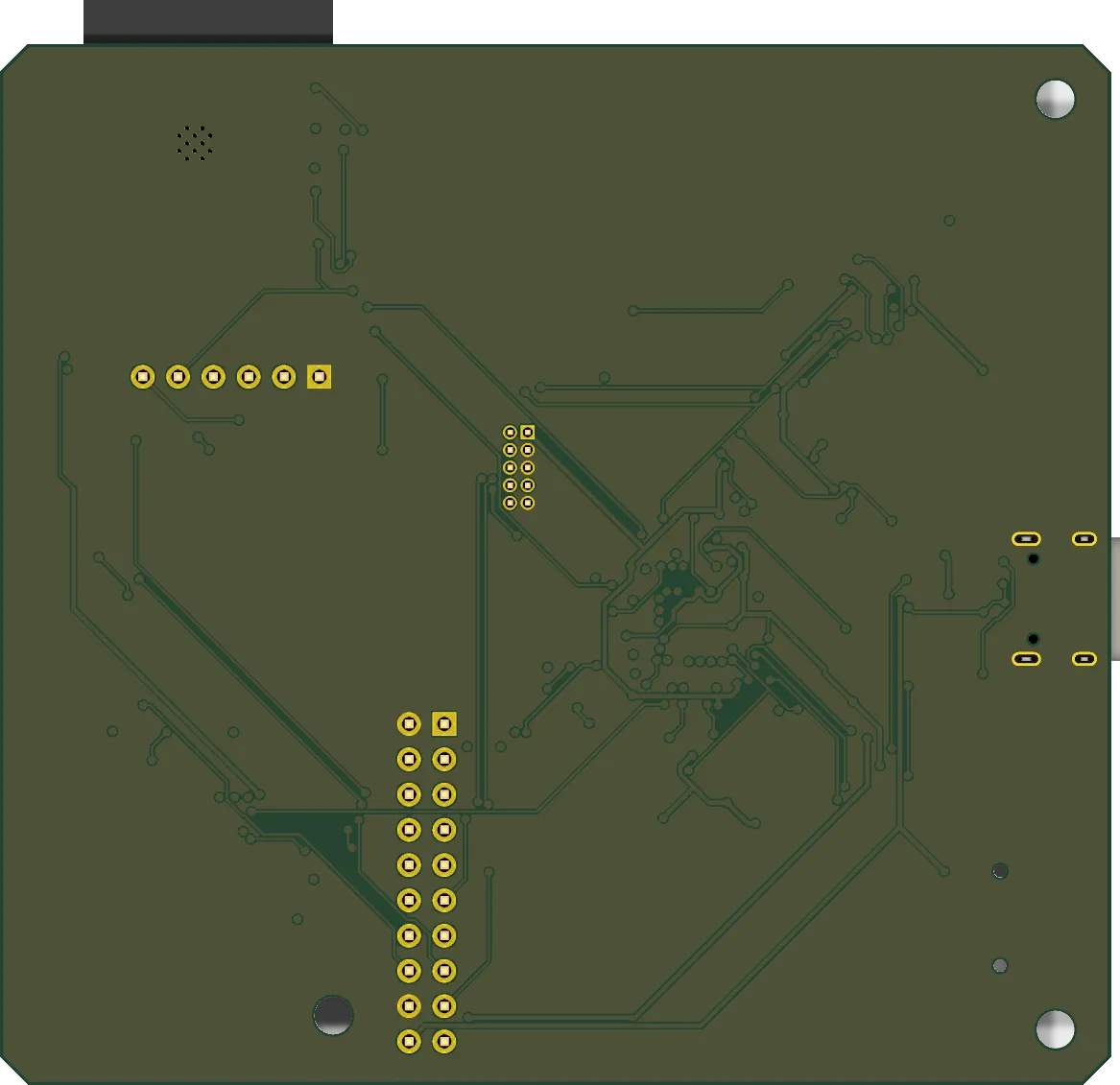
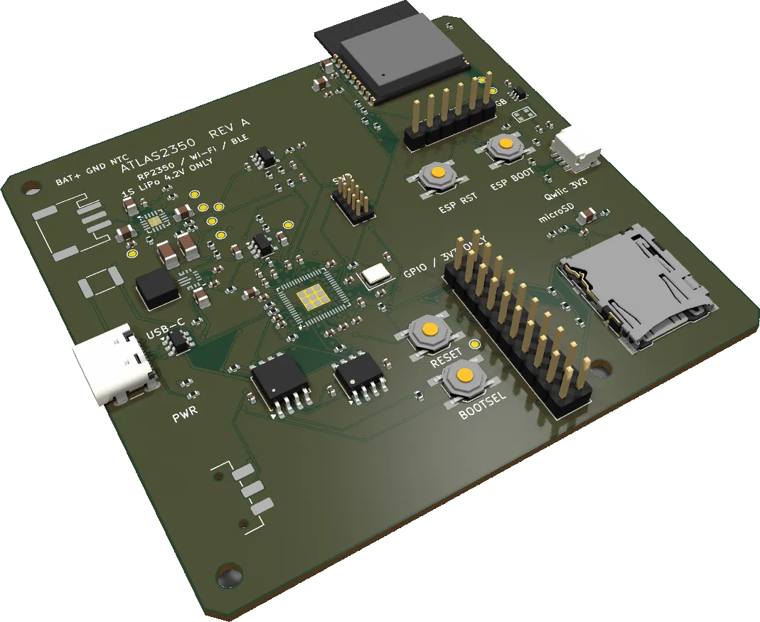
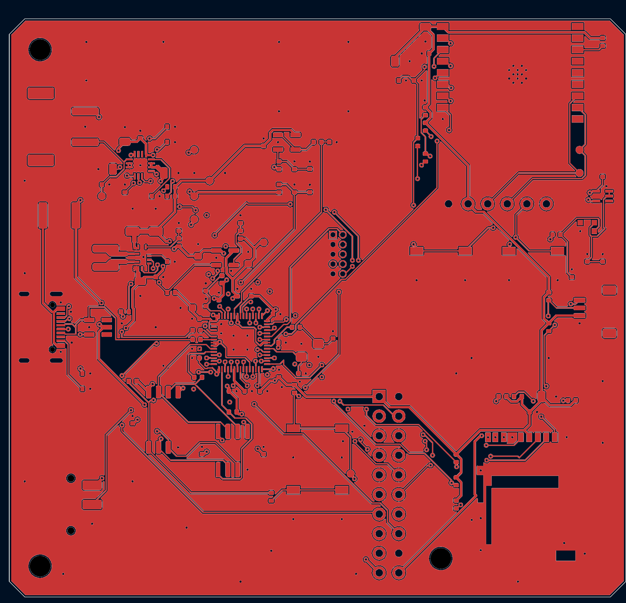
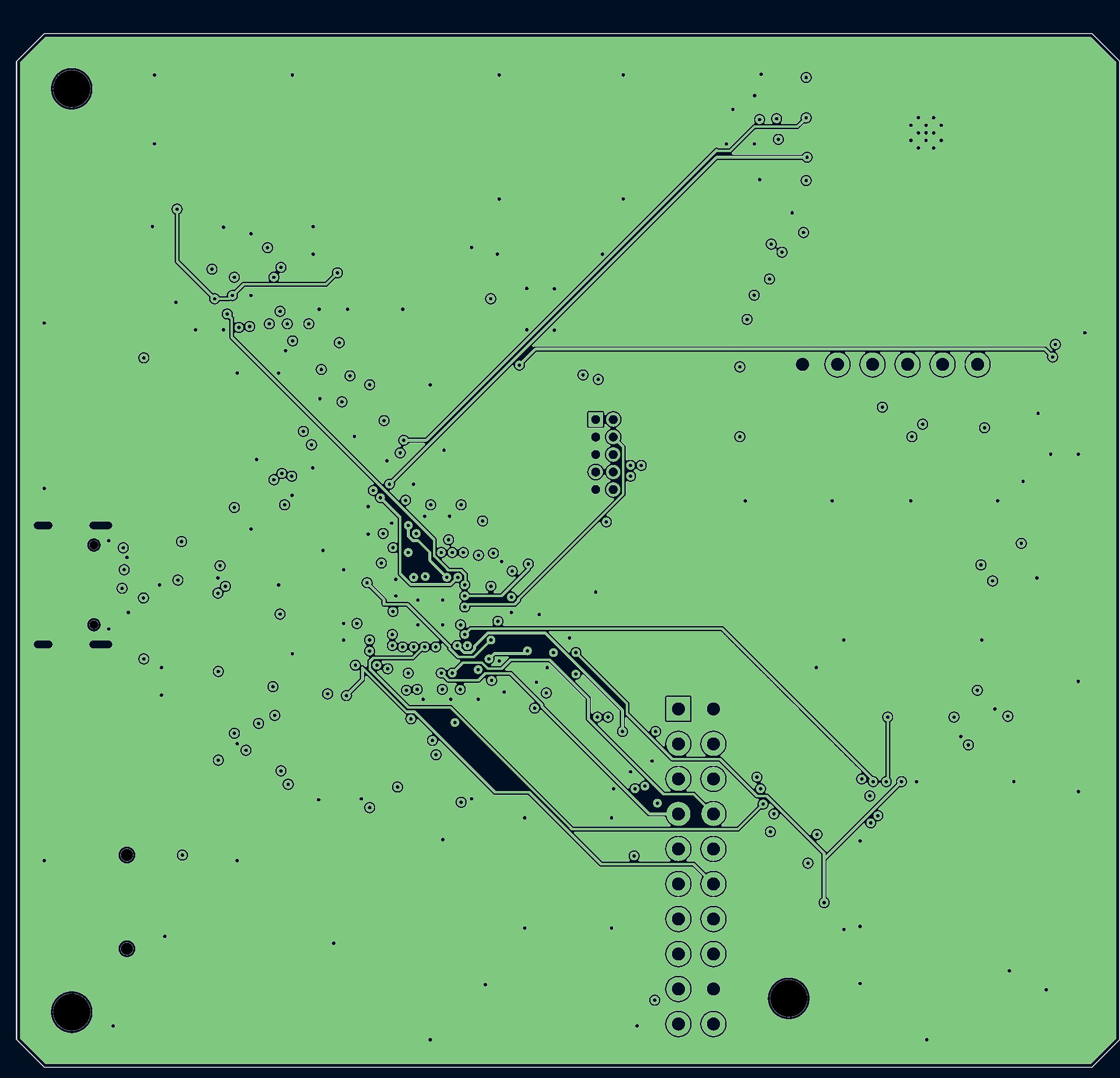
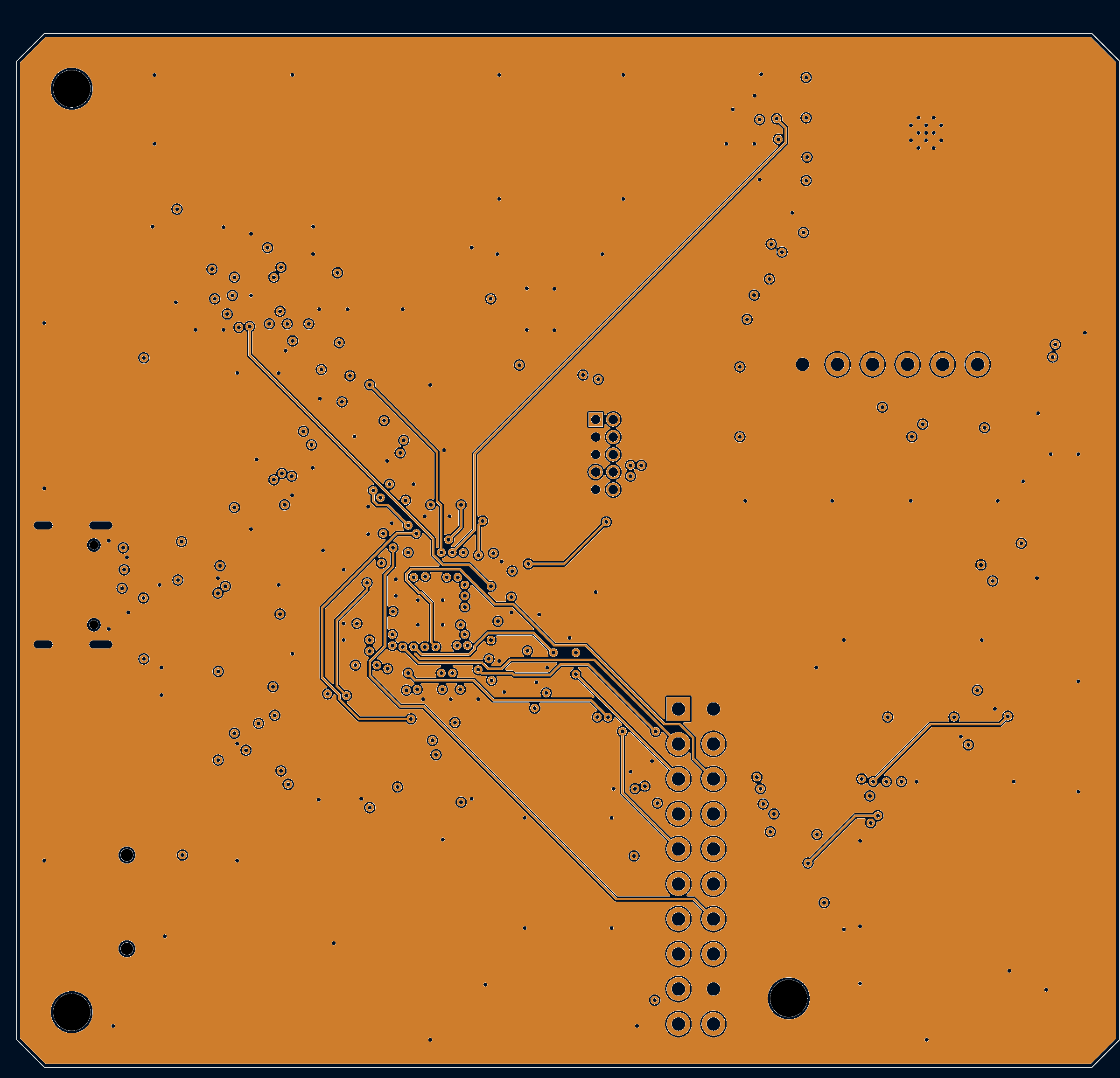
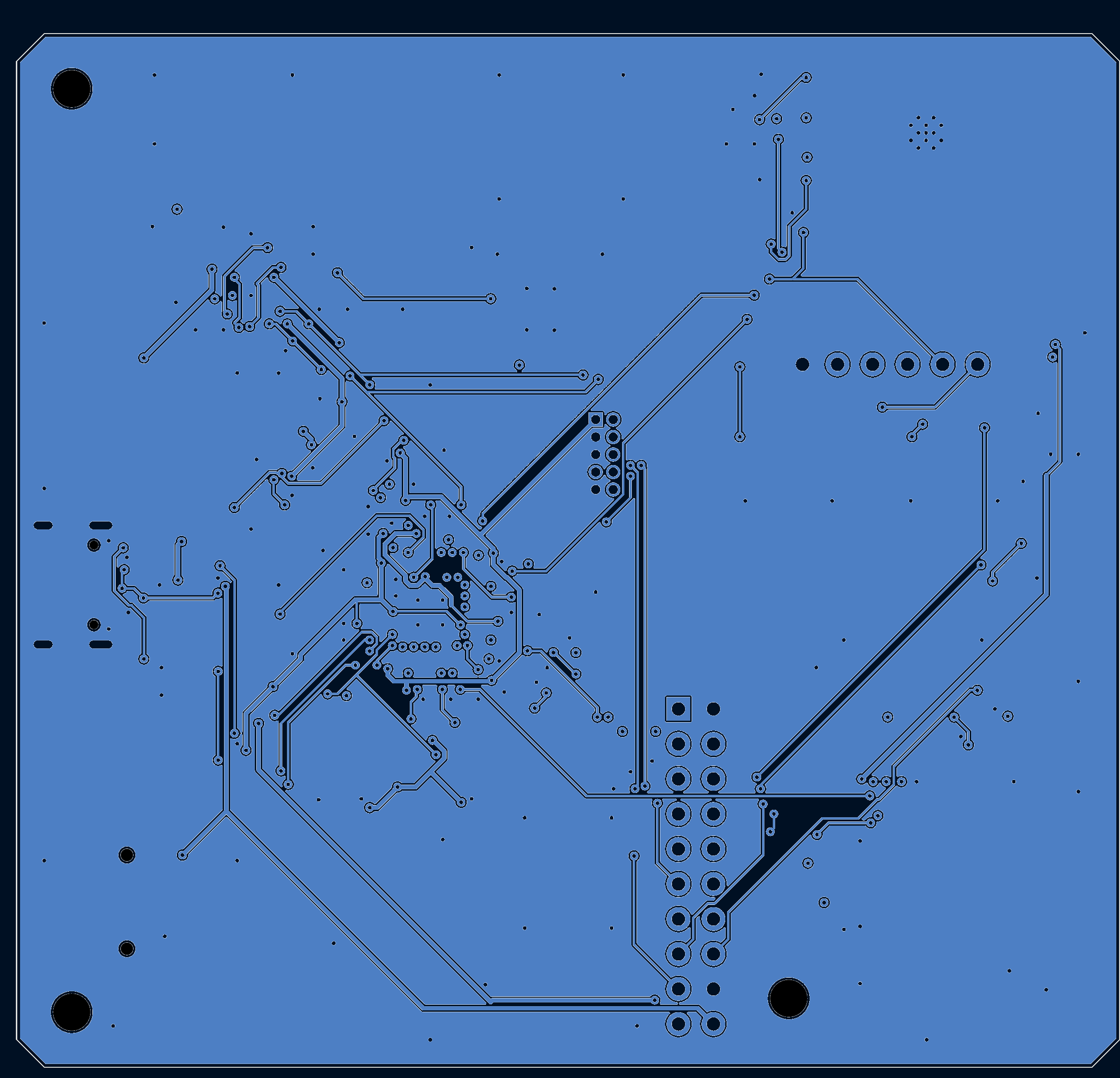
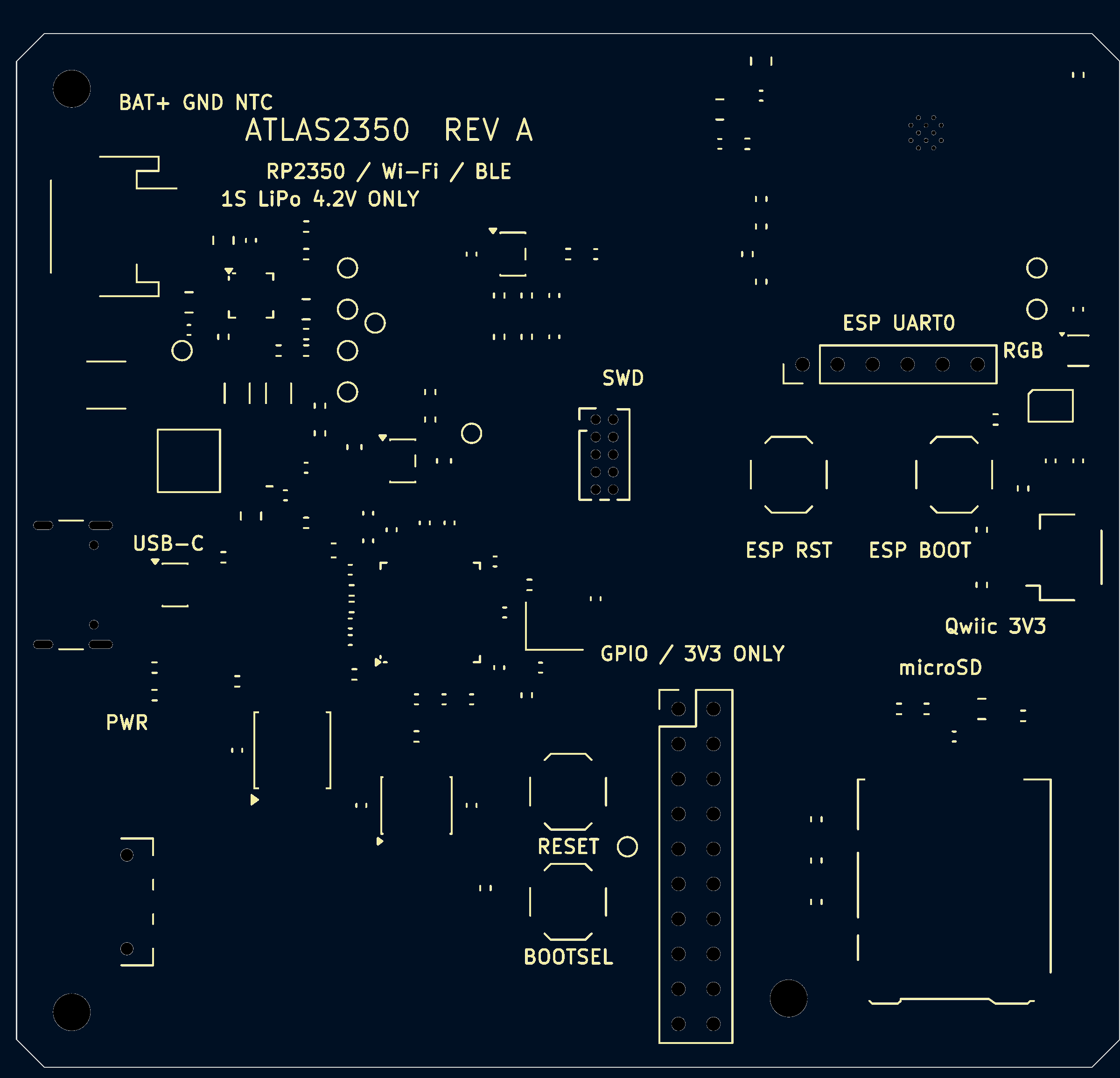
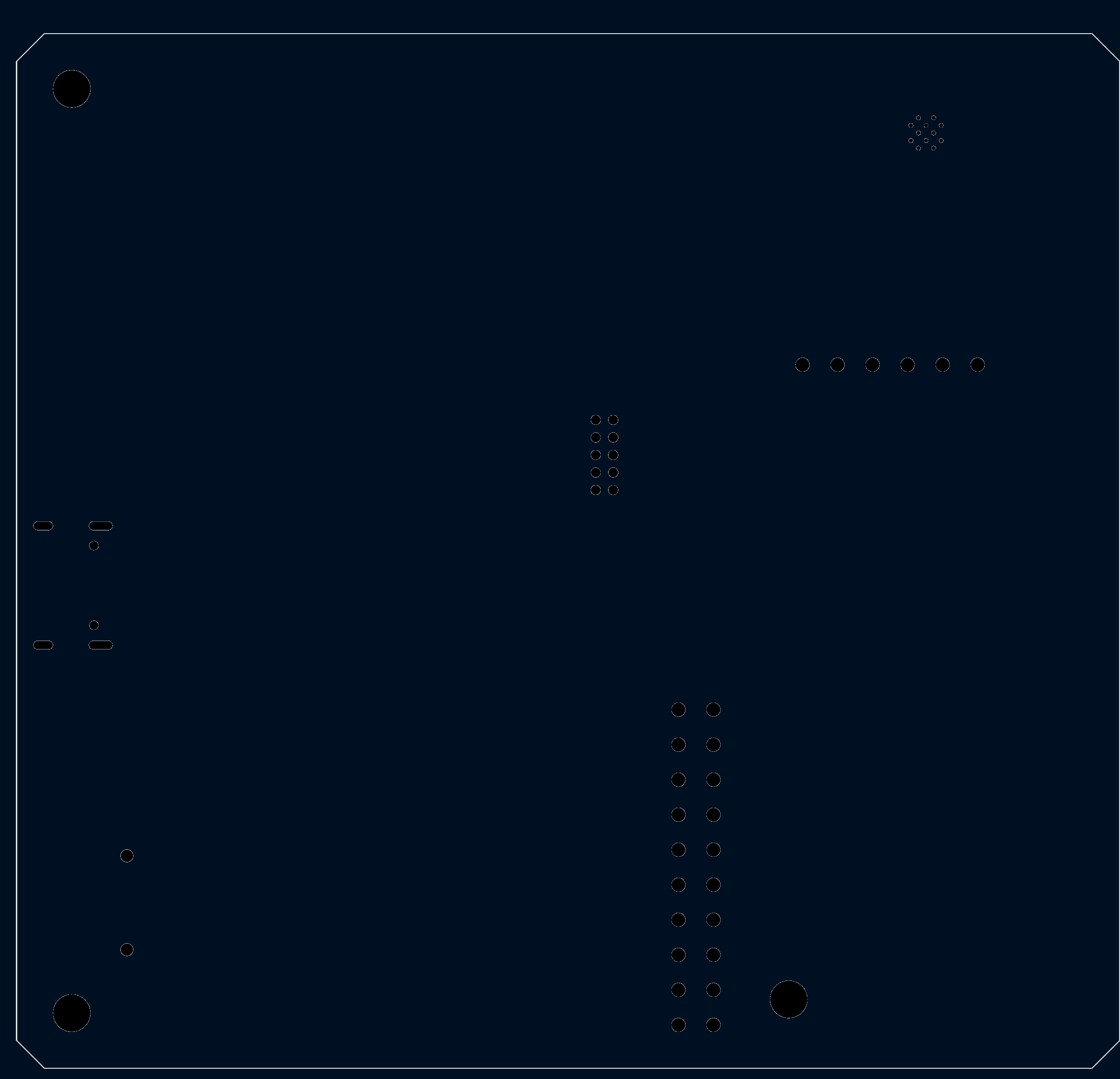
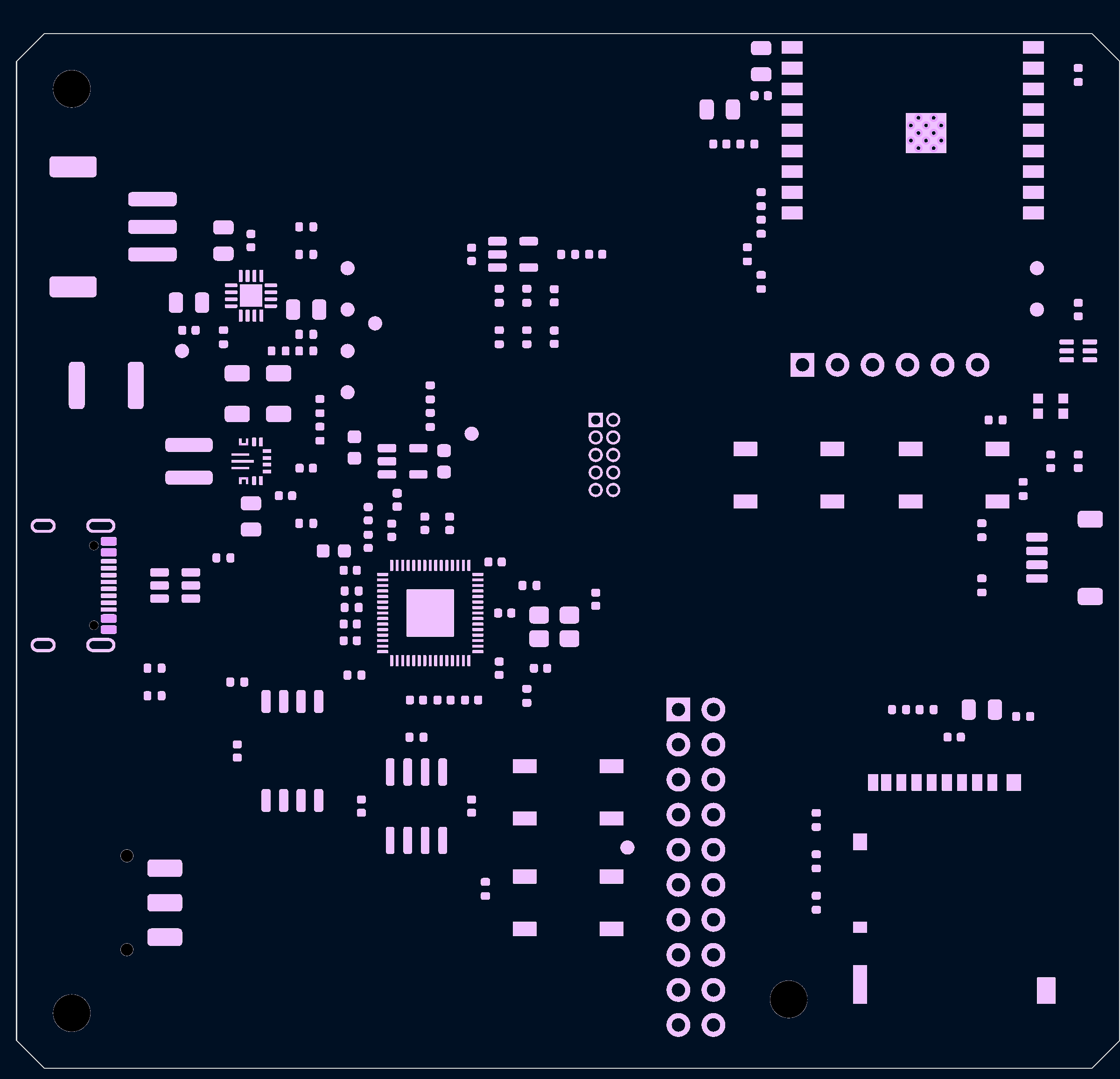
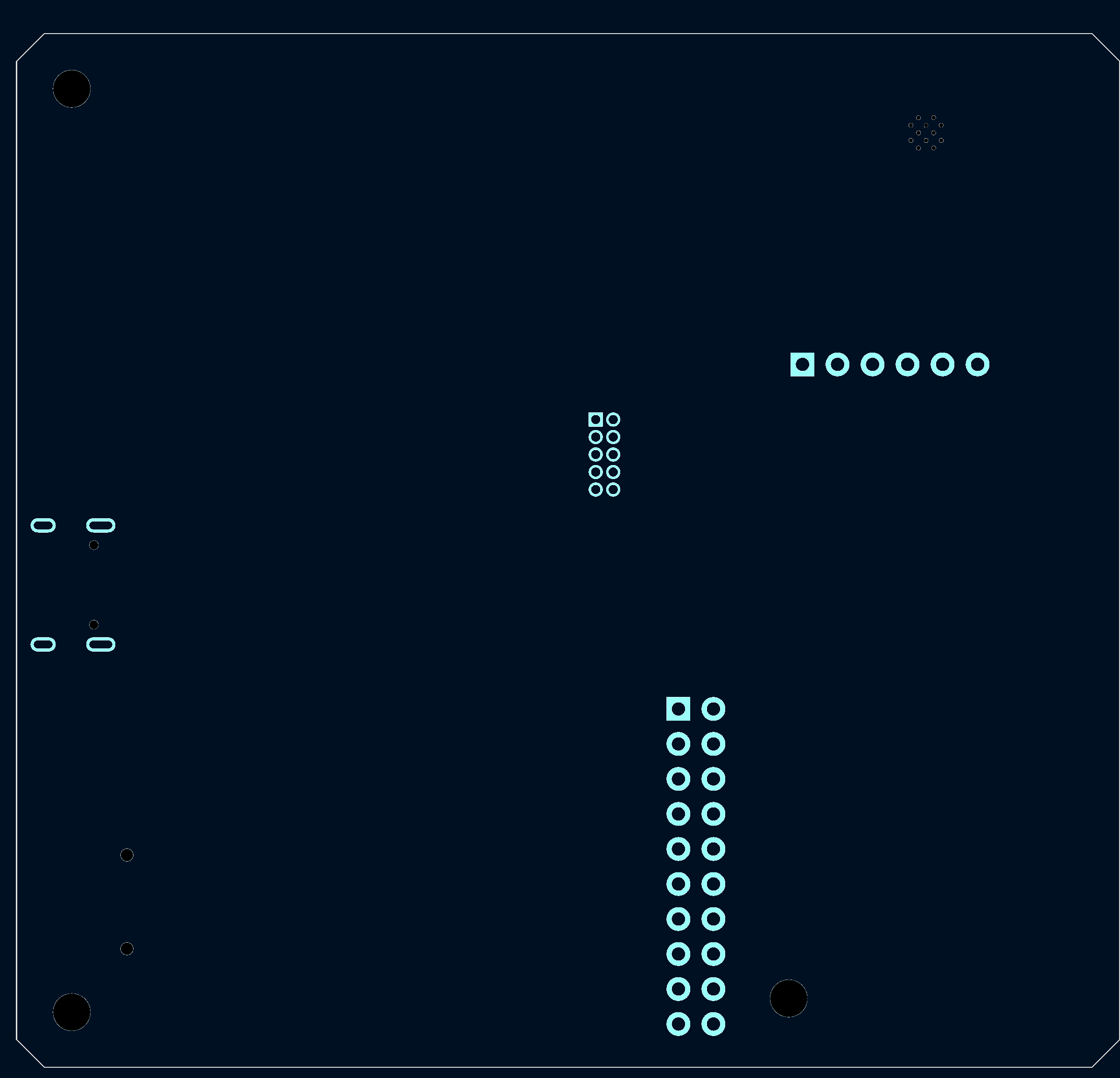
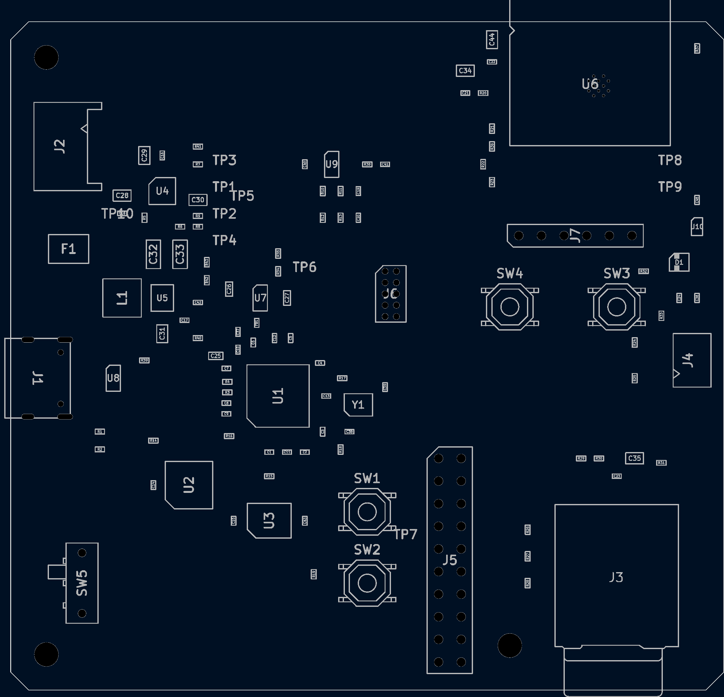
Rendered by kicad-cli with the run's own KiCad version. Dimensions in mm. The layers are the plots the AI judge saw, seen from the top, with their white background made dark. Click one to open it at full size.
- AI cost
- $14.36
- Time
- 1 h 36 min
- Tokens, incl. cache reads
- 52.4M
- 1 board
- $297.32
- 5 boards, per board
- $87.53
- Board size
- 80 × 75 mm
- Machine
- EC2 Mac (mac2-m2)
- chatgpt
- 26.1103.60933
- codex
- codex-cli 0.167.0-alpha.3.2
- kicad
- 10.99.0-6353-g0ef63a79e8
- texttocad
- cad 0.11.4
- texttocadKicad
- 10.99.0-6305-g5ac898839d (kicode 10.99.0.dev20261106)
Score
Design review11 of 20
- Layout8 of 101 minus 0.1 per minor and 0.2 per major layout finding, down to 0
- Routing3 of 10the same, for routing findings
Circuit checks20 of 20
- Decoupling5 of 5RP2350 power pins with a capacitor within 3.2 mm
- USB protection5 of 50.5 for an ESD part on D+ and D−, plus 0.25 for each line with a series resistor
- Antenna keepout5 of 51 when there are keepouts and no copper is in them
- Battery drain5 of 51 at 5 µA or less drawn by unswitched battery dividers, falling linearly to 0 at 25 µA
Layout checks16.7 of 30
- Thermal pads3.2 of 10mean over the exposed pads of their vias over the number needed, 0 for a pad with no plane on another layer
- Grounding8.5 of 10USB, QSPI and microSD track length over a ground plane on the next layer
- Silkscreen5 of 5texts at least 0.8 mm high
- Board size0 of 51 at the Feather RP2350's 50.8 × 22.8 mm area or less, falling linearly to 0 at 5 times that area
Orderable4 of 20
- Fab notes0 of 51 when every fab option in the notes can be ordered from PCBWay
- Board0 of 51 when the board needs no rework
- BOM lines4 of 101 minus 0.2 for each BOM line that needs a fix, down to 0
Parts data4.7 of 10
- 3D models4.7 of 5parts with a 3D model
- Supplier part numbers0 of 5BOM lines with a valid number from at least one supplier
| The five groups | 56.4 |
|---|---|
| Every gate passed, so no penalty | 0 |
| Score | 56.4 of 100 |
Gates
A board that fails a gate loses 20 points. The gates are the three checks below, every prompt feature, and any fatal review finding.
| Check | Result | What the check found |
|---|---|---|
| Crystal and load capacitors | Pass | Y1 ABM8-272-T3 (CL 10 pF) between XIN and XOUT via R17 1k 1%; load caps XIN: C38 15pF 50V C0G; XTAL_OUT: C39 15pF 50V C0G; needs 10.5–17.5 pF per side for 3 pF stray |
| BOOTSEL and RUN buttons | Pass | QSPI_SS (FLASH_CS) → R19 → SW2 → GND; RUN (RUN) → SW1 → GND |
| Charger power path | Pass | U4 BQ24074RGTR: U4 IN (VBUS) is on J1 VBUS; BAT (VBAT) goes to J2; U5 TPS63070RNMR makes +3V3 from OUT (VSYS) |
Prompt features
- Found RP2350 U1
- Found QSPI flash U2
- Found PSRAM U3
- Found USB-C J1
- Found Wi-Fi and BLE U6
- Found microSD J3
- Found Qwiic J4
- Found RGB LED D1
- Found Power-path charger U4
- Found Battery monitoring R38
Design review 11 of 20
Opus 5.5 reviewed an anonymous copy of the board and listed 7 findings. Layout and routing each start at 10 points.
Major
Routing
The battery path from the LiPo connector to the charger's BAT pins is a 0.15 mm trace, mostly on a 0.5 oz inner layer, but it carries up to 1.5 A.
Evidence
J2 pad 1 (9.85, 12.00) runs on F.Cu at 0.15 mm to via (11.635, 12.74), then on In1.Cu (17.5 um copper per the stackup) at 0.15 mm through (11.635, 16.51), (14.365, 19.24) and (15.41, 19.24) to via (15.65, 19.00), and only then widens to 0.3 mm into U4 pads 2/3 (15.562, 18.75/19.25). The copper cross-section is 0.0026 mm2, far below what 1.5 A needs (about 0.5 mm of 1 oz outer copper for a 10 C rise per IPC-2221).
The charger output to the buck-boost input is a 0.3 mm trace with single 0.3 mm vias, but it carries up to 1.5 A.
Evidence
From C30 pad 1 (20.05, 20.00) the VSYS track is 0.3 mm: F.Cu to via (19.63, 21.06), B.Cu through (23.595, 25.025) and (23.595, 28.47) to via (19.955, 32.11), then F.Cu through (19.02, 33.50) and (17.55, 33.50) to U5 VIN pads 12/13 (16.225-16.725, 32.40). The run is about 15 mm long. IPC-2221 gives about a 25 C rise for 0.3 mm of 1 oz outer copper at 1.5 A. About 0.5 mm is needed for 10 C.
Minor
Layout
The flash and PSRAM sit about 10 mm and 12 mm from the QSPI pins, and the PSRAM is chained behind the flash, so the QSPI runs reach 27-28 mm.
Evidence
The U1 QSPI pins 55-60 are at x = 26.55, y = 42.8-44.8. U2's centre (20.0, 52.0) is 9.7 mm from U1 pad 60, and U3's centre (29.0, 56.0) is 11.9 mm from U1 pad 59. QSPI_IO2 runs U1 pad 58, then U2 pad 3, then U3 pad 3, for 28.3 mm of track. QSPI_IO1 is 27.1 mm long.
The side-actuated power slide switch sits back from the left edge, so its actuator ends 4.2 mm inside the board outline instead of reaching the edge.
Evidence
SW5 (C&K JS102011SAQN, a right-angle SMT part per the C&K JS datasheet) is at (8.0, 63.0) rotated -90. Its F.Fab actuator (local x -2 to -0.5, y 1.8 to 3.8) maps to board x 4.2-6.2, y 61.0-62.5, and the body spans x 6.2-9.8. The Edge.Cuts line is at x = 0.
Routing
QSPI_IO1 has 4 vias, two of them for a needless 1.6 mm hop onto F.Cu, and QSPI_IO0 has 3 vias.
Evidence
QSPI_IO1 has vias at (27.25, 44.40), (26.13, 45.825), (24.57, 45.825) and (19.695, 54.47). Between the 2nd and 3rd via it runs on F.Cu (26.13, 45.825) to (24.57, 45.825), then returns to B.Cu. QSPI_IO0 has vias at (27.25, 43.60), (22.555, 47.905) and (30.42, 52.325). QSPI_IO3 and QSPI_CLK are routed with no vias.
USB D+ and D- are not routed as a pair. D- changes layer through 4 vias, and D+ detours around U8, so it is 4.3 mm longer.
Evidence
USB_D- has vias at (7.65, 40.25), (7.80, 38.90), (9.20, 40.95) and (14.60, 40.60), with B.Cu between them. USB_D+ stays on F.Cu but runs from U8 pad 1 (10.363, 39.05) up to (10.363, 37.40), across to (12.40, 37.40) and back down at x = 13.8 to y = 41.6, about 3.5 mm away from D- at y = 40.95. Track lengths are D+ 26.8 mm and D- 22.5 mm.
SD_MOSI and SD_CS each change layer 5 times on their way to the microSD socket.
Evidence
SD_MOSI has vias at (34.255, 45.37), (37.05, 44.785), (42.12, 49.595), (57.395, 60.19) and (62.465, 56.745), and uses F.Cu, In1.Cu, B.Cu and In2.Cu. SD_CS has vias at (32.695, 44.395), (33.475, 46.15), (46.345, 50.635), (58.045, 58.11) and (61.945, 57.265). SD_CLK covers the same distance with 2 vias.
Opus 5.5's notes
I wrote review.json with 7 findings. Two are major and five are minor. I found no fatal faults.
The two major problems are both power traces too thin for the 1.5 A you set for the charger output and battery path:
| Area | Severity | Refs / net | Problem |
|---|---|---|---|
| routing | major | J2→U4, VBAT |
The battery path is a 0.15 mm trace. About 9 mm of it runs on In1.Cu, which is only 17.5 µm (0.5 oz) copper. It goes through 3 vias and only widens to 0.3 mm at U4's BAT pads. |
| routing | major | U4→U5, VSYS |
The charger output to the buck-boost input is a 0.3 mm trace, about 15 mm long, with single 0.3 mm-drill vias. By IPC-2221 that's roughly a 25 °C rise at 1.5 A. About 0.5 mm is needed for 10 °C. |
| layout | minor | U2, U3 | The flash is 9.7 mm and the PSRAM 11.9 mm from the QSPI pins. The PSRAM is wired after the flash, so QSPI_IO1 and QSPI_IO2 run 27–28 mm. |
| routing | minor | QSPI_IO1, QSPI_IO0 |
IO1 has 4 vias, two of them for a pointless 1.6 mm hop onto F.Cu. IO0 has 3 vias. |
| routing | minor | USB_D+, USB_D- |
The two lines aren't routed as a pair. D- uses 4 vias. D+ detours around U8 and ends up 4.3 mm longer. |
| routing | minor | SD_MOSI, SD_CS |
Each changes layer 5 times. SD_CLK covers the same distance with 2. |
| layout | minor | SW5 | The power switch is a side-actuated part (C&K datasheet), but its actuator ends 4.2 mm inside the board edge instead of reaching it. |
Upgrade: I upgraded all six schematics in place from format 20250114 to 20261106 (10.99). The board was already in the connector's format, so kicad-cli pcb upgrade left it unchanged. ERC and DRC both report 0 violations after the upgrade.
What passed:
- Placement: the parts listed in your brief are where they should be:
- The antenna hangs off the top edge with nothing in front of it.
- USB-C, the LiPo connector, Qwiic and microSD all open toward their edges.
- The crystal is about 5 mm from XIN/XOUT, with short traces.
- The charger and regulator sit together near the power input.
- Fatal faults: two subagents checked every part's pin mapping and footprint against its datasheet. All pads match the stock KiCad footprints. Board nets match the schematic. The custom TPS63070 footprint matches TI's land pattern. The feedback dividers give 3.30 V and 1.10 V. The ESP32 boot pins, UART crossover, SD-in-SPI and Qwiic pinouts are all correct.
Left out:
- Tactile buttons away from the edge, since they're pressed from above.
- VBUS at 0.3 mm, since its input current limit is set to about 0.5 A.
I deleted my scratch files and the board.kicad_prl that kicad-cli created. The folder now holds only the upgraded design and review.json.
Subagent report 1
Task: You are helping review an RP2350 development board KiCad project in /home/ubuntu/review (files: board.kicad_pcb, *.kicad_sch, libraries/Atlas.pretty footprints, libraries/Atlas.kicad_sym, bom.csv). The board is already upgraded; DO NOT modify any project file. Write scratch files only under /home/ubuntu/review/scratch/. Read and write only in /home/ubuntu/review, the KiCad connector and its libraries ($SPROCKET_KICAD_LIBRARIES). Read datasheets on the web as needed. Nobody will answer questions.
I found no fatal faults in the power section. I checked every in-scope part against both the board/schematic files and the datasheets, and none of them stops the board from working or damages a part. The report is in /home/ubuntu/review/scratch/other_power.md.
Three part roles in the brief are wrong. The netlist shows:
- R5/R6 are not the buck-boost feedback divider. R5 (3.57k) sets the BQ24074 charge current (ISET) and R6 (3.24k) sets its input current limit (ILIM).
- R42/R43 are not a battery divider. R42 (312k, +3V3→MAIN_FB) and R43 (100k, MAIN_FB→GND) set the TPS63070 output.
- The battery divider is R10/R11 (470k/470k), buffered by U9. The VBUS divider is R12/R13 (1M/330k).
How I checked
- Nets: the schematic netlist matches the PCB pad nets. The only exceptions are the unconnected J2/J4 mounting pads.
- Footprints: every Atlas footprint that has a stock KiCad equivalent has the same pads as stock. The footprints placed on the board match the library, and no part is mirrored.
- Copper: each power net is one connected piece of copper, GND included.
Checked and OK
| Part | Result | Evidence |
|---|---|---|
| U5 TPS63070, custom footprint | Pad numbers and positions match the TI RNM0015A land pattern (datasheet p.39). | Pins 1–4 run down the left side, 5–8 along the bottom, 9–11 are the long bars on the right, 12–15 along the top. Positions match the drawing, including the bridged 7/8 and 12/13 pads. The board rotates the part 180°, which puts pin 1 at (18.15, 31.75). |
| U5 pin nets | Match the datasheet pin table (§6). | PS/SYNC and EN go to PWR_EN. PG goes to MAIN_PG with a 10k pull-up. VAUX has 100 nF. FB2 and VSEL are on GND, which the datasheet allows when unused. VOUT is +3V3, VIN is VSYS, L1/L2 go to the inductor. |
| U5 output | 3.3 V | 0.8 V × (1 + 312k/100k) = 3.296 V. The 1k series resistor on EN and PS/SYNC follows §8.4. The 1.0 µH inductor is within the allowed range. |
| U4 BQ24074 | All 16 pins plus the exposed pad match Fig. 7-2 / Table 7-1. | CE is on GND, so charging is on. EN1/EN2 go to GPIO16/17 with 100k pull-downs. TMR and ITERM are open, which gives the default timers and 10 % termination. |
| U4 resistors | Within the datasheet ranges (§8.3). | Charge current 890/3.57k = 249 mA. Input limit ≈ 0.47–0.50 A. VSYS stays at or below 4.5 V. |
| J1, R1/R2, F1 | OK | VBUS and GND pins are correct. Each CC pin has its own 5.1k to GND, so the board only gets 5 V. F1 sits between the connector and the rest of VBUS. |
| U8 USBLC6-2SC6 | Pinout matches the ST datasheet (DS4260). | Pin 1 D+, 2 GND, 3 D−, 5 VBUS after the fuse. Pins 4/6 are the internal duplicates of 3/1 and are left open. |
| U7 TLV75801P | SOT-23-5 pinout matches Fig. 4-2. | IN=+3V3, GND, EN=MAIN_PG, FB=CORE_FB, OUT=+1V1. |
| U7 divider | 1.10 V | R34 is the top resistor (+1V1→FB) and R35 the bottom (FB→GND). 0.55 V × (1 + 10k/10k) = 1.10 V, below the RP2350 core maximum of 1.21 V. |
| RP2350 core supply | Wired as the datasheet's external-supply circuit (p.410, Fig. 24). | VREG_FB is on GND and VREG_LX is open. The internal regulator's inputs are on 3V3. U7 is enabled by the 3V3 power-good, so the core comes up after the I/O supply. |
| U9 TLV9001IDBVR | Pinout matches Fig. 6-1. | Unity-gain buffer of VBAT/2 (at most 2.1 V), powered from 3V3, so the ADC0 pin stays at or below 3.3 V. With 3V3 off, input current is about 9 µA, far below the 10 mA limit. |
| VBUS_ADC (ADC1) | Stays below the ADC limit. | 5 V gives 1.24 V at the pin. With the power switch off and USB connected, the pin can only feed about 5 µA into the unpowered chip, which isn't a damage case. |
| U10 TPS22919 | Pinout matches the datasheet. | It switches VSYS to the WS2812 LED supply. All its pins stay at or below 4.5 V, under the 6 V maximum. |
| SW5 JS102011SAQN | Can't short VSYS to GND. | It only drives the 3V3 regulator and LED switch enables through 1k. It is a non-shorting type ("N" suffix), so VSYS and GND are never bridged when it moves. It does not disconnect the battery. |
| J2 JST PH 3-pin | Footprint numbering is correct. | Pin 1 VBAT, 2 GND, 3 NTC. There is no standard pin order for 3-pin battery packs with a thermistor, so I can't call this a fault. |
| U6 ESP32-C3 | Power pins OK. | Pin 1 is on +3V3 with 22 µF and 10 µF, pins 9 and 19 are GND. |
| Capacitor voltage ratings | All exceed their rail voltage. |
Not fatal, worth knowing
- At power-up the charger limits USB input to 100 mA, because the pull-downs hold EN1/EN2 low. Firmware has to drive GPIO16/17 to raise the limit.
- The battery pack's wire order must match J2's pin order (VBAT, GND, NTC).
My scripts, the downloaded datasheets and page renders are in scratch/, next to the report.
Subagent report 2
Task: You are helping review an RP2350 development board KiCad project in /home/ubuntu/review (files: board.kicad_pcb, *.kicad_sch, libraries/Atlas.pretty footprints, libraries/Atlas.kicad_sym, bom.csv). The board is already upgraded; DO NOT modify any project file. Write scratch files only under /home/ubuntu/review/scratch/. Read and write only in /home/ubuntu/review, the KiCad connector and its libraries ($SPROCKET_KICAD_LIBRARIES). Read datasheets on the web as needed. Nobody will answer questions.
I found no fatal faults in the digital/IO section. Every in-scope pin, net, footprint and boot pin matches the datasheets. The report is in scratch/other_digital.md; its content follows.
How it was checked
- Footprints: all 34 footprints in
libraries/Atlas.prettyhave the same pads as the stock KiCad 10 versions: numbers, positions, sizes and rotations. The board's footprints match those library files. Everything is on F.Cu atscale 1 1, so nothing is mirrored. - Nets: the board's pad nets match the schematic netlist on all 432 pads. The only exceptions are the J2 and J4 mounting pads, which have no net in either file.
- Fitting: no part is marked DNP. Only test points, mounting holes and power flags are left out of the BOM.
Checked and OK
| Part | Checked against | Result |
|---|---|---|
| U1 RP2350A pins | Datasheet Tables 1674–1679, Fig. 2 | All GPIOs on the right pins. IOVDD (1, 11, 20, 30, 38, 45), USB_OTP_VDD (53) and QSPI_IOVDD (54) on +3V3. DVDD (6, 23, 39) on +1V1. ADC_AVDD (44) through FB1. Pad 61 on GND. XIN to Y1.1, XOUT through R17 1k to Y1.3. SWCLK 24, SWDIO 25, RUN 26 with a 10k pull-up. |
| U1 package | Datasheet top view | Pad 1 at (27.20, 45.45) and pad 60 at (26.55, 44.80) are side by side at one corner. Pads number counter-clockwise. Pad 61 is the 3.4 mm "reduced ePad" the datasheet shows. |
| U1 core regulator pins with U7 | §6.3.7, Fig. 24 (p. 409) | VREG_AVDD and VREG_VIN on +3V3, PGND on GND, LX unconnected, FB on GND. This is exactly Fig. 24. U7's R34/R35 (10k/10k, 0.55 V feedback) gives 1.1 V. |
| USB | Table 1678 | Pin 52 → R3 27Ω → J1 A6/B6 (D+). Pin 51 → R4 27Ω → J1 A7/B7 (D−). |
| U2 W25Q32JV / U3 APS6404L | W25Q32JV §3.3, APS6404L pin table | All four data lines go to the same pins on both chips (SD0→pin 5, SD1→2, SD2→3, SD3→7). Clock goes through R16 33Ω to pin 6. QSPI_SS → U2.1 and GPIO0 → U3.1, each with a 10k pull-up. Pins number counter-clockwise. Package sizes are right (SS 208 mil, SN 150 mil). |
| PSRAM CS on GPIO0 | RP2350 Table 3 | GPIO0 function F9 is the second memory chip select (QMI CS1n). |
| U6 ESP32-C3-WROOM-02 | Module datasheet Table 3-1, §3.1 | All 19 pads match. Pads 1–9 run down the left side, 10–18 up the right. |
| U6 boot pins | Table 4-3 | IO9, IO8 and IO2 each have a 10k pull-up to 3.3 V, so it boots from flash. GP19 can pull IO9 low through 1k for download mode. |
| U6 EN | "Do not leave EN floating" | EN has a 10k pull-down, and GP18 drives it high through 1k (about 3.0 V; the high threshold is 2.475 V). The schematic note says the pull-down is intentional. |
| UART to the ESP32 | RP2350 Table 3; ESP-AT C3 default pins | GP20 is UART1 TX → ESP IO6 (RX). ESP IO7 (TX) → GP21, UART1 RX. ESP IO4 (RTS) → GP22, UART1 CTS. GP23, UART1 RTS → ESP IO5 (CTS). Every line is crossed correctly. |
| J3 microSD | Hirose pinout; RP2350 SPI1 | CS → GP13 (CSn), MOSI → GP11 (TX), VDD on pin 4, CLK → GP10 (SCK), GND on pin 6, MISO → GP12 (RX). All card lines have 47k pull-ups. Card detect: pin 9 → GP15 with a 10k pull-up, pin 10 to GND. |
| J4 Qwiic | Qwiic pin order; RP2350 I2C0 | Pins are GND, 3.3 V, SDA (GP4), SCL (GP5), with 4.7k pull-ups. |
| D1 WS2812B-2020-V6 | V6 datasheet | Pin 1 DOUT, 2 GND, 3 DIN (from GP14 through 330Ω), 4 power from VSYS through U10. Its input threshold is 0.55 × VDD, so 2.9 V even at 5.3 V, which 3.3 V logic clears. |
| Y1 crystal | ABM8 pinout | Pins 1 and 3 go to the RP2350 crystal pins, 2 and 4 to GND. |
| J6 SWD header | Cortex 10-pin pinout | 3.3 V, SWDIO, GND, SWCLK, GND, NC×3, GND, RUN, all on the right pins. |
| J5, J7 | Wrong nets or shorted rails | None found. |
| SW1–SW4 | TL3342 drawing P010632 | Pads with the same number are the pairs joined inside the switch, so it only closes between pads 1 and 2. SW1 RUN, SW2 BOOT (through 1k to QSPI_SS), SW3 ESP boot and SW4 ESP enable each switch to GND. None shorts a power rail. |
Not fatal, but firmware has to handle them
- The ESP32-C3 stays off until RP2350 firmware drives GP18 high.
- The RP2350's internal regulator still starts with FB on GND and LX unconnected. Firmware should turn it off (set VREG.HIZ = 1) to save about 400 µA. The datasheet calls leaving it on "a safe mode of operation".
The helper scripts I wrote and the downloaded datasheets are also in scratch/.
Circuit checks 20 of 20
Decoupling
5 of 514 of 14 RP2350 power pins have a capacitor within 3.2 mm.
| Pin | Pad | Net | Nearest capacitor | Distance |
|---|---|---|---|---|
| IOVDD | 1 | +3V3 | C9 | 2.91 mm |
| DVDD | 6 | +1V1 | C11 | 3.14 mm |
| IOVDD | 11 | +3V3 | C2 | 3.14 mm |
| IOVDD | 20 | +3V3 | C3 | 2.79 mm |
| DVDD | 23 | +1V1 | C13 | 1.47 mm |
| IOVDD | 30 | +3V3 | C4 | 1.18 mm |
| IOVDD | 38 | +3V3 | C5 | 2.93 mm |
| DVDD | 39 | +1V1 | C12 | 2.57 mm |
| ADC_AVDD | 44 | ADC_AVDD | C10 | 2.45 mm |
| IOVDD | 45 | +3V3 | C6 | 2.07 mm |
| VREG_AVDD | 46 | +3V3 | C7 | 1.89 mm |
| VREG_VIN | 49 | +3V3 | C7 | 2.4 mm |
| USB_OTP_VDD | 53 | +3V3 | C8 | 2.03 mm |
| QSPI_IOVDD | 54 | +3V3 | C8 | 1.91 mm |
USB protection
5 of 5- ESD parts on D+ and D−
- U8
- D+ nets, connector to RP2350
- USB_D+ → USB_PHY_D+ series resistor
- D− nets, connector to RP2350
- USB_D- → USB_PHY_D- series resistor
Differential pair, not scored
- D+ and D− length
- 28.51 mm and 24.53 mm
- Mismatch
- 3.98 mm
- Vias
- 4
- Longest coupled stretch
- 8.29 mm on F.Cu, 0.15 mm wide, 0.15 mm gap
- Differential impedance
- 95.5 Ω
Antenna keepout
5 of 51 keepout covers the Wi-Fi module U6.
| Keepout | Layers | Copper inside |
|---|---|---|
| U6 footprint | F.Cu, B.Cu, In1.Cu, In2.Cu | none |
Battery drain
5 of 5Unswitched dividers draw 4.47 µA from a full battery, even when the board is off.
| Divider | Buffered by | Switched by | At 4.2 V |
|---|---|---|---|
| R10 470k / R11 470k | U9 | none | 4.47 µA |
Layout checks 16.7 of 30
Thermal pads
3.2 of 10| Exposed pad | Net | Vias | Needed | Plane on another layer |
|---|---|---|---|---|
| U1 | GND | 4 | 9 | yes |
| U4 | GND | 1 | 5 | yes |
Grounding
8.5 of 10| Bus | Over ground | Track length | Share |
|---|---|---|---|
| USB | 48.7 mm | 53 mm | 91.9% |
| QSPI | 140.2 mm | 157.3 mm | 89.1% |
| microSD | 194.4 mm | 242.2 mm | 80.3% |
| All three | 383.3 mm | 452.5 mm | 84.7% |
Silkscreen
5 of 50 of 16 texts are below PCBWay's 0.8 mm minimum. The smallest is 1 mm.
Board size
0 of 580 × 75 mm, 6000 mm². The Feather RP2350 is 50.8 × 22.8 mm.
Orderable 4 of 20
| 1 board | 5 boards | |
|---|---|---|
| PCBs | $156.77 | $156.77 |
| Assembly | $88.00 | $112.84 |
| Components | $52.55 | $168.02 |
| Total | $297.32 | $437.63 |
| Per board | $297.32 | $87.53 |
PCBWay's instant quote for the options in the fab notes, without shipping. PCBWay makes at least 5 PCBs, so 1 board is 5 PCBs with 1 assembled. Parts are at distributor list prices. The prices include the fixes below.
Fixes made to price the order
| Area | Parts | Problem | Fix |
|---|---|---|---|
| Fab notes | The fab notes ask for 0.5 oz inner copper, which PCBWay does not offer | Quoted 1 oz inner copper | |
| BOM | C26, C27 | Invalid MPN: Murata makes no GRM188R61A225KE15D | Priced GRM188R61A225KE34D, the 2.2uF 10V X5R 0603 |
| BOM | R42 | Unavailable part: no 312k 0.1% 0402 is sold by LCSC, DigiKey or Mouser | Priced RT0603BRD07312KL, the same series in 0603 |
| Board | R42 | The 0402 footprint doesn't fit the 0603 substitute | Assumed a 0603 footprint; not re-quoted, since the PCB is at PCBWay's minimum price and the part count is unchanged |
Fab notes
0 of 5- The fab notes ask for 0.5 oz inner copper, which PCBWay does not offer
Board
0 of 5- R42: The 0402 footprint doesn't fit the 0603 substitute
BOM lines
4 of 103 of 53 BOM lines need a fix.
- C26, C27: Invalid MPN: Murata makes no GRM188R61A225KE15D
- R42: Unavailable part: no 312k 0.1% 0402 is sold by LCSC, DigiKey or Mouser
- not stocked for 5 boards: C29
Parts data 4.7 of 10
3D models
4.7 of 57 parts have no 3D model the run's KiCad can load: D1, F1, J2, SW5, U1, U4, U5.
Supplier part numbers
0 of 50 of 53 BOM lines have a valid supplier part number.
LCSC 0%, Digi-Key 0%, Mouser 0%
Stock
98.1% of 53 BOM lines are stocked for 5 boards at LCSC, JLCPCB or Digi-Key.
| Parts | MPN | Needed |
|---|---|---|
| C29 | GRM21BR61A475KA73L | 5 |
| Parts | MPN | At |
|---|---|---|
| C25 | GRM188R60J475KE19D | Digi-Key |
| C28, C30, C31, C35, C44 | GRM21BR61A106KE19L | Digi-Key |
| C29 | GRM21BR61A475KA73L | Digi-Key |
| C32, C33 | GRM31CR61C226KE15L | LCSC, Digi-Key |
| C36, C37, C43, C45 | GRM155R61A105KE15D | Digi-Key |
| U2 | W25Q32JVSSIQ | Digi-Key |
DRC and ERC
| Errors | Warnings | Unconnected | |
|---|---|---|---|
| DRC | 0 | 0 | 0 |
| ERC | 0 | 0 |
Files
The agent's README
Atlas2350 Rev A
Atlas2350 is an 80 × 75 mm RP2350A development board with 4 MiB QSPI flash, 8 MiB QSPI PSRAM, an ESP32-C3 Wi-Fi/BLE UART coprocessor, microSD, USB-C, and an external protected single-cell LiPo power path. Documentation reflects the final owner decisions on 2026-11-10. The saved native PCB and assembly exports from that board are authoritative for positions, rotations and pads; design.json and placement scripts can contain earlier coordinates. These documents describe the current choices; earlier alternatives in research.md are not the assembly specification.
Status: complete prototype CAM package. The final revision includes U10/C45 for switched LED power; checks/verification.json is PASS with all 432 declared pin assignments checked, 115 components / 128 footprints, and final ERC/DRC each report zero errors. Final CAM parse is PASS: 10 Gerbers, 374 PTH, 7 NPTH, and 334 filled/capped holes registered within a 0.00051 mm export-rounding tolerance. All QSPI including FLASH_CS remains F/B only. Use the matching final source/export hashes and verification reports for the order. This is a prototype first-article package, with no supplier quote/stock commitment, DFM approval or physical/functional testing claimed. Initial quote quantity is five completely assembled boards.
Final population is 115 components / 128 footprints / 53 BOM groups, with 13 bare H/TP features excluded. All 432 declared pin assignments pass the published verification. Intentional U6/J3/J6 footprint edits remain part of the released local library.
Fabrication has not started. The initial quote quantity is five completely assembled prototype boards, each with all 115 real BOM components fitted. No supplier quote, PCBWay stock commitment, supplier DFM approval or assembled-board functional testing is established. This package is for prototype first articles, not mass-production approval. Order only after final verification/export review and supplier capability/quote confirmation.
Native file compatibility
Release archives: PCBWay manufacturing/assembly ZIP and complete KiCad source plus manufacturing files. The manufacturing ZIP includes a file manifest and SHA-256 checksums; the complete source archive also retains design-generation tools and review evidence.
The PCB was generated by KiCad 10.99.0 development, native PCB format 20261031. Use a compatible KiCad 11 development/nightly build that supports this format; stable KiCad 9/10 are not compatible project editors. The schematic format is 20250114; that older schematic version does not make the newer PCB compatible with stable releases. Keep the native format intact and use the CAM/PDF exports for suppliers who do not have the compatible development build.
No application firmware binary or preloaded ESP-AT image is promised. Blank RP flash and an ESP module without the required application are expected unless the owner supplies programming images and instructions. PCBWay must still populate and solder every released BOM part, including all through-hole parts. Firmware-dependent factory functional testing is optional and requires owner-supplied firmware, fixtures and acceptance limits.
Documentation
- Assembly notes: exact packages, component pins, header orientation, complete population and process notes.
- Fabrication notes: stackup, geometry, mandatory filled/capped routing vias and mechanical requirements.
- Test plan: first-article inspection, power/charge tests, programming and optional functional qualification.
- Primary-source research: verified manufacturer URLs and electrical evidence, including historical alternatives. Primary-source verification date: 2026-11-10.
The complete prototype delivery uses the following fab/ layout; confirm all files share the final U10-revision source/export identity:
- fab/README.md and fab/order-instructions.md: package identity and prototype order instructions.
- fab/gerbers/ and fab/drill/: final copper/mask/outline CAM and plated/NPTH drill data.
- fab/assembly/: bom.csv,
parts.csv, placement.csv, kicad-native-position.csv,assembly-pinout.csv,top-assembly-orientation.svg,assembly-orientation.mdandmanifest.json, generated from the saved final PCB. - Reconcile filled-capped-hole-schedule.csv with the final drill data: 322 routing vias + twelve U6 0.30 mm thermal PTH features = 334 resin-filled/copper-capped holes. Total PTH is 374, comprising the 334 filled/capped features and 40 open component lead/shell holes. Total NPTH is 7, unplated and unfilled. Fill/cap every routing via and all twelve module thermal holes, never component lead/shell holes. The final schedule and drill classification govern processing.
- Assembly orientation PDF and KiCad top assembly PDF: supplier-readable assembly drawings.
- fab/schematic.pdf: supplier-readable schematic.
- fab/fabrication-notes.md, fab/assembly-notes.md, and fab/test-plan.md: copies of the matching source notes.
PCBWay must assemble all 115 real component references in 53 BOM groups. The 128 footprint objects include 13 excluded bare H/TP features; these are not DNP components. No customer-soldered or DNP component population is planned. Exact MPN stock and lead times cannot be guaranteed without a supplier quote. No firmware has been built or provided, and no customer application/ESP-AT binary is included.
Preferred placement.csv uses millimetres, X right and positive Y down, at the saved KiCad footprint anchor, not a physical-body centroid. kicad-native-position.csv uses the native exported Y-negative convention. PCBWay must reconcile origin, rotation and machine setup against actual pin1 positions in assembly-pinout.csv and the assembly drawings; the two placement formats do not share the same Y convention.
The generated pcbway-centroids.csv contains 112 surface-mounted physical F.Fab body-box centers, including U10/C45, hybrid SMT/THT J1 and surface-mounted U6 with thermal holes; pure THT J5/J6/J7 are excluded. The generated centroid-source.csv retains all 115 component centers for review/manual THT placement. Centroid CSV coordinates are mm, X right and Cartesian Y=−boardY. These are body-box centers, not anchors, courtyards or centers of mass; reconcile rotation/origin with actual pin1 coordinates and assembly drawings. PCBWay specifies surface-mounted parts only in the centroid file.
Assembly drawing floorplan/clearance envelopes are courtyard envelopes, not physical body edges; use generated F.Fab body-center data for centroid review and manufacturer drawings for mechanical verification.
Final hardware decisions
| Function | Selected implementation |
|---|---|
| Main MCU | U1 RP2350A, QFN60 with GND exposed pad61 |
| Boot flash | U2 W25Q32JVSSIQ, wide 5.3 mm SOIC8, 4 MiB |
| PSRAM | U3 APS6404L-3SQR-SN, narrow SOIC8, 8 MiB; shared QSPI, separate select on GP0 |
| Charger / power path | U4 BQ24074RGTR; USB100/USB500/suspend controlled by GP16/17 |
| Main regulator | U5 TPS63070RNMR, custom exact RNM0015A footprint; R42 312 kΩ / R43 100 kΩ, both 0.1%, nominal 3.296 V |
| Main inductor | L1 XAL4020-102MEC, 1.0 µH, stock Coilcraft XAL4020 land pattern |
| Main output capacitors | C32/C33 GRM31CR61C226KE15L, each 22 µF, 16 V, X5R, 1206; combined effective-capacitance target >22 µF |
| Core regulator | U7 TLV75801PDBVR, 1.1 V from 10 kΩ/10 kΩ feedback; enabled by MAIN_PG |
| Battery measurement | R10/R11 470 kΩ 1%, U9 TLV9001IDBVR unity buffer, R38 100 Ω and C41 1 nF ADC filter |
| Radio | U6 ESP32-C3-WROOM-02-N4; AT UART1 with CTS/RTS; UART0 download on J7 |
| LED | D1 WS2812B-2020-V6, powered by LED_VDD via U10 TPS22919DCKR from VSYS, direct 3.3 V data through R32 330 Ω; no shifter or dedicated boost |
| LED power switch | U10 TPS22919DCKR, SC70-6; IN=VSYS, ON=PWR_EN, VOUT/QOD=LED_VDD; C45 1 µF at input |
| Battery connector | J2 JST S3B-PH-SM4-TB(LF)(SN), custom three-wire pack assignment |
| USB | J1 GCT USB4105-GF-A, USB2 device/sink, separate 5.1 kΩ CC resistors |
| microSD | J3 Hirose DM3AT-SF-PEJM5, SPI mode plus detect |
| I²C | J4 SM04B-SRSS-TB(LF)(SN), horizontal JST SH; 3.3 V |
| SWD | J6 FTSH-105-01-L-D, through-hole 1.27 mm 2×5 header; no -DV suffix |
Coilcraft's primary XAL40xx table confirms XAL4020-102MEC: ±20% inductance, 13.25 mΩ typical / 14.60 mΩ maximum DCR, 8.7 A Isat at 30% typical inductance drop, and 6.7/9.6 A reference currents for 20/40 °C rise. These are reference measurements requiring thermal derating, not universal safe operating currents. Primary Coilcraft PDF, Document806 revised 02/25/26.
Complete RP2350A physical pinout
Names and net assignments below use U1 pad numbers, not header numbers. +3V3 is nominally 3.296 V; ADC_AVDD is supplied through FB1. Spare GPIO nets are brought to J5 where listed in the assembly notes.
| Pad | RP name | Actual net / function |
|---|---|---|
| 1 | IOVDD | +3V3 |
| 2 | GPIO0 | PSRAM_CS, QMI CS1n |
| 3 | GPIO1 | GPIO1 |
| 4 | GPIO2 | GPIO2 |
| 5 | GPIO3 | GPIO3 |
| 6 | DVDD | +1V1 |
| 7 | GPIO4 | I2C_SDA, I²C0 |
| 8 | GPIO5 | I2C_SCL, I²C0 |
| 9 | GPIO6 | GPIO6 |
| 10 | GPIO7 | GPIO7 |
| 11 | IOVDD | +3V3 |
| 12 | GPIO8 | GPIO8 |
| 13 | GPIO9 | GPIO9 |
| 14 | GPIO10 | SD_CLK, SPI1 SCK |
| 15 | GPIO11 | SD_MOSI, SPI1 TX |
| 16 | GPIO12 | SD_MISO, SPI1 RX |
| 17 | GPIO13 | SD_CS, software select |
| 18 | GPIO14 | RGB_DATA, PIO |
| 19 | GPIO15 | SD_DETECT, low when inserted |
| 20 | IOVDD | +3V3 |
| 21 | XIN | XIN, Y1 pin1 |
| 22 | XOUT | XOUT → R17 1 kΩ → XTAL_OUT/Y1 pin3 |
| 23 | DVDD | +1V1 |
| 24 | SWCLK | SWCLK, J6 pin4 |
| 25 | SWDIO | SWDIO, J6 pin2 |
| 26 | RUN | RUN, J6 pin10 / SW1 |
| 27 | GPIO16 | USB_500_EN → BQ EN1 |
| 28 | GPIO17 | USB_SUSPEND_EN → BQ EN2 |
| 29 | GPIO18 | ESP_EN_CTRL → R22 → ESP_EN |
| 30 | IOVDD | +3V3 |
| 31 | GPIO19 | ESP_BOOT_CTRL → R23 → ESP_BOOT |
| 32 | GPIO20 | WIFI_TX, UART1 TX → ESP GPIO6 RX |
| 33 | GPIO21 | WIFI_RX, UART1 RX ← ESP GPIO7 TX |
| 34 | GPIO22 | WIFI_CTS, UART1 CTS ← ESP GPIO4 RTS |
| 35 | GPIO23 | WIFI_RTS, UART1 RTS → ESP GPIO5 CTS |
| 36 | GPIO24 | CHARGE_N, BQ open-drain status |
| 37 | GPIO25 | POWERGOOD_N, BQ input-power status |
| 38 | IOVDD | +3V3 |
| 39 | DVDD | +1V1 |
| 40 | GPIO26 / ADC0 | BAT_ADC, buffered VBAT/2 |
| 41 | GPIO27 / ADC1 | VBUS_ADC, unbuffered VBUS divider |
| 42 | GPIO28 / ADC2 | GPIO28_ADC2 |
| 43 | GPIO29 / ADC3 | GPIO29_ADC3 |
| 44 | ADC_AVDD | ADC_AVDD, FB1-filtered +3V3 |
| 45 | IOVDD | +3V3 |
| 46 | VREG_AVDD | +3V3, external-core configuration |
| 47 | VREG_PGND | GND |
| 48 | VREG_LX | NC |
| 49 | VREG_VIN | +3V3, external-core configuration |
| 50 | VREG_FB | GND |
| 51 | USB_DM | USB_PHY_D−, via R4 27 Ω |
| 52 | USB_DP | USB_PHY_D+, via R3 27 Ω |
| 53 | USB_OTP_VDD | +3V3, required supply |
| 54 | QSPI_IOVDD | +3V3 |
| 55 | QSPI_SD3 | QSPI_IO3 |
| 56 | QSPI_SCLK | QSPI_CLK_SRC → R16 33 Ω → QSPI_CLK |
| 57 | QSPI_SD0 | QSPI_IO0 |
| 58 | QSPI_SD2 | QSPI_IO2 |
| 59 | QSPI_SD1 | QSPI_IO1 |
| 60 | QSPI_SS | FLASH_CS; SW2 branch through R19 1 kΩ |
| 61 | Exposed GND | GND |
Power and firmware contract
J1 nominal 5 V enters VBUS_RAW, passes F1 to VBUS, then U4 supplies VSYS. U5 supplies +3V3; MAIN_PG releases U7's +1V1 core supply. SW5 controls PWR_EN through R39, enabling U5 and U10 together. U10 disconnects and discharges LED_VDD when SW5 is off, preventing D1's latched color from remaining illuminated. The battery, charger and upstream VSYS remain connected. U5 PS/SYNC shares PWR_EN, so an enabled regulator uses automatic PWM/PFM power-save behavior.
| GP16 / EN1 | GP17 / EN2 | Input mode |
|---|---|---|
| 0 | 0 | USB100 at reset, approximately 90–100 mA |
| 1 | 0 | USB500 after host configuration permits it, approximately 450–500 mA |
| 0 | 1 | Resistor-programmed ILIM mode; avoid accidental selection |
| 1 | 1 | USB suspend |
R7/R41 100 kΩ pull-downs select USB100 at reset. Firmware must handle host configuration, reset, suspend and resume; no complete USB policy is supplied. In suspend without a battery, the system can lose power and revert to reset defaults. R5 3.57 kΩ programs about 250 mA nominal charge current; system load consumes the same input budget. DPPM reduces charge before battery supplementation. ITERM is NC (default 10%, 3.3% in USB100); TMR is NC (nominal 30 min precharge / 5 h fast charge).
Use an external protected 500 mAh 1S 4.2 V LiPo with a cell-mounted 10 kΩ NTC and the custom J2 pin order. Pack, cable, SD card and debug adapters are not supplied board components. The approximately 0–50 °C charge window depends on the actual NTC curve/tolerances; confirm the pack specification. No fixed TS bypass or board-ambient substitute is fitted. BQ24074 is not a battery protection IC.
The main rail targets operation down to BAT 2.8 V after startup, subject to power-path drop, load and qualification. TPS63070 cold startup requires SYS/VIN ≥3.0 V while VOUT is below 3.0 V. A deeply discharged pack is not guaranteed to cold-start the board at 2.8 V; this is an accepted component limitation requiring test, not a full-range startup promise. Core LDO heating and minimum-input regulator stability remain first-article qualification items.
Firmware must set RP POWMAN VREG.HIZ using the protected register-write mechanism for the external-core supply; initialize shared QMI flash/PSRAM with separate chip selects, PSRAM startup/reset and bounded transactions; configure the actual SPI1/I²C0/UART1 pin assignments; and leave ESP reset low until the power budget permits radio operation. ESP-AT UART1 defaults are GPIO6RX/7TX/5CTS/4RTS, normally 115200 baud, but depend on the flashed binary. No factory ESP-AT image is assumed.
For first-article bring-up, start QSPI at ≤31.25 MHz and SD SPI at ≤12.5 MHz after the card's required slower initialization sequence. These are conservative firmware recommendations pending signal-integrity qualification, not measured bus-speed guarantees. QSPI and hand-routed USB use F/B copper; no controlled-impedance claim is made. Higher bus clocks require first-article waveform/error-rate and concurrent-load validation.
RGB uses VSYS-derived LED_VDD through U10, with direct 3.3 V GPIO data, using the primary PDF's VIH=0.55×VDD. The owner accepts that the LED may fall outside its guaranteed supply range at low battery; the system rail's operating range does not guarantee RGB operation. Firmware shall blank conservatively at BAT ≤3.6 V under load, with calibration/hysteresis and sag assessment. Firmware blanking at low battery does not disconnect D1; SW5 off disables U10 and discharges LED_VDD through QOD. Use GRB data and a reset-low interval >280 µs; budget approximately 36 mA for full white. No 5 V LED boost or AHCT shifter is part of this design.
U10 pin map: 1 IN=VSYS, 2 GND, 3 ON=PWR_EN, 4 NC floating, 5 QOD=LED_VDD, 6 VOUT=LED_VDD. D1/C24/C36 use LED_VDD; C45 adds 1 µF from VSYS to GND at U10 input. QOD tied directly to VOUT enables internal output discharge. The main rail remains 3.296 V. This switch supplies no boost/regulation: RGB remains outside its guarantee if LED_VDD falls below 3.3 V. Primary TI TPS22919 datasheet.
U10 schematic model: local symbol pin5 QOD is typed passive to represent TI's explicitly permitted direct tie to VOUT/pin6 (LED_VDD). The stock open_collector type produces an ERC conflict with the power-output pin6 for this permitted connection. Only the schematic electrical type is changed: pin numbers, package pinout and footprint are unchanged. No ERC exclusions are used. TI TPS22919 pin-functions table.
Mechanical and fabrication target
Four layers: F/B signals, power and full GND pours; In1/In2 predominantly stitched GND pours with low-speed escape corridors on both inner layers. The inner layers are not continuous GND planes. Ground connectivity includes the outer pours and exposed-pad link. Construction is 1.6 mm, ENIG, outer 1 oz / inner 0.5 oz copper; signal width 0.15 mm, clearance 0.127 mm, routing via 0.60 mm land / 0.30 mm finished hole. Every routing via requires IPC-4761 Type VII resin fill and copper cap, including ground decoupler/EP vias and the twelve 0.30 mm radio thermal holes. Component lead holes remain open. No controlled impedance is specified or claimed; see the fabrication notes for return-path and supplier review.
The native PCB now encodes the requested nominal stackup, replacing default finish/copper/dielectric metadata: ENIG; outer copper 35 µm, inner copper 17.5 µm; dielectric gaps 0.120 / 1.255 / 0.120 mm from front to back. Copper plus dielectrics total 1.600 mm excluding soldermask coatings, nominal 0.010 mm each side. Green soldermask and white silkscreen are selected. This is the requested construction, not an unspecified default stock stackup; the supplier must quote actual materials, cured dielectric thickness and finished tolerances. No controlled-impedance order or qualification is claimed. See the nominal layer table in the fabrication notes. J6's ten open finished PTH lead holes are 0.70 mm with 1.00 mm copper lands, nominal 0.15 mm annular ring; do not fill/cap them.
U6 placement origin is (65,7) mm, with antenna overhang approximately 6.1 mm beyond top Edge.Cuts y=0. Its antenna copper keepout lies outside the PCB; maintain antenna clearance in the panel, assembly fixture and enclosure. Three 2.7 mm M2.5 NPTH mounting holes are centered at (4,4), (4,71), (56,70) mm. They are mechanical features, not DNP parts.