Rank 4 of 7 in RP2350 dev board
Fable 5.2 in Backplane
Anthropic's Fable 5.2 on medium reasoning, in Backplane hub driving Claude Code.
68.4 of 100
 76.222.86
 76.222.86
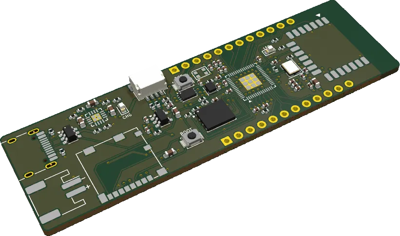
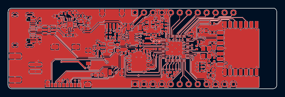
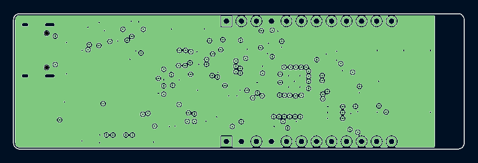
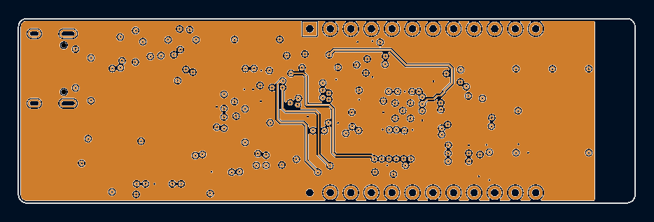
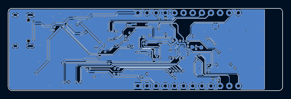
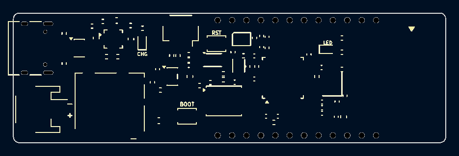
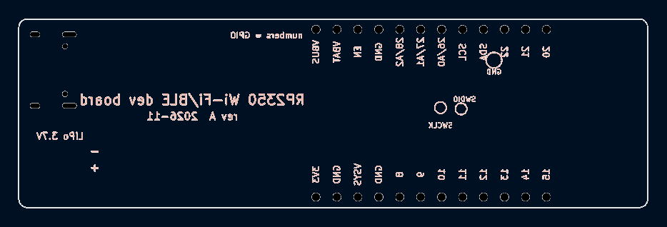
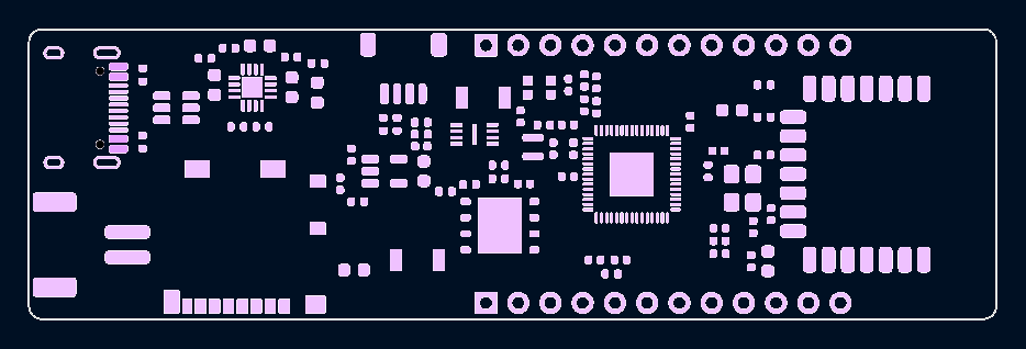
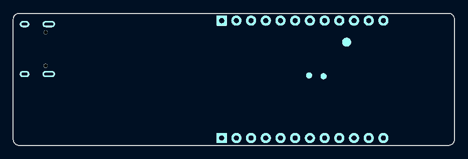
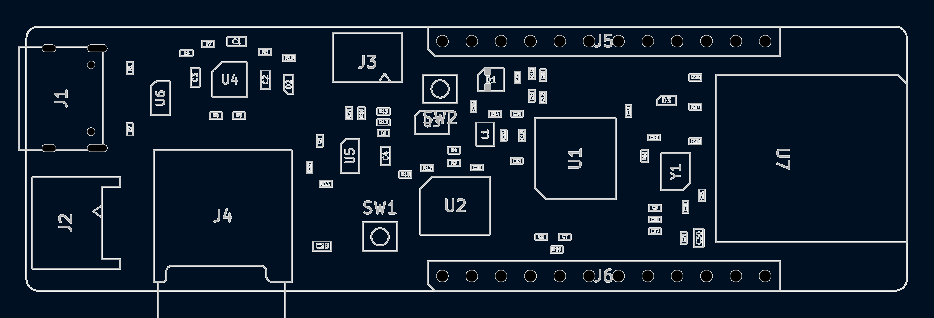
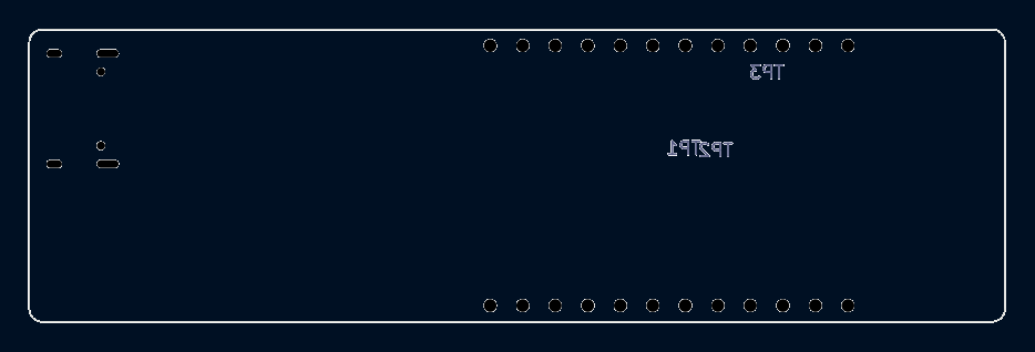
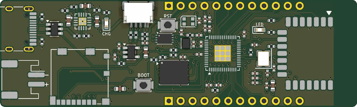
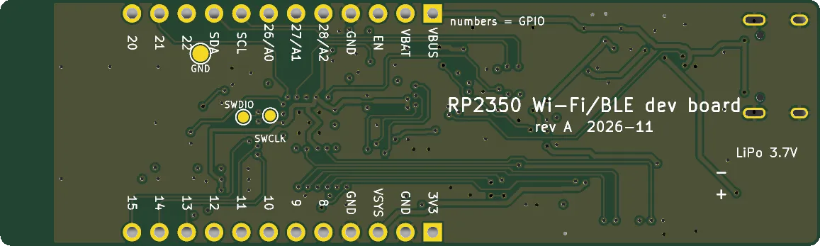
Rendered by kicad-cli with the run's own KiCad version. Dimensions in mm. The layers are the plots the AI judge saw, seen from the top, with their white background made dark. Click one to open it at full size.
- AI cost
- $49.09
- Time
- 3 h 45 min
- Tokens, incl. cache reads
- 55.6M
- 1 board
- $187.53
- 5 boards, per board
- $52.68
- Board size
- 76.2 × 22.86 mm
- Machine
- EC2 Ubuntu (c7i.2xlarge)
- backplane
- backplane-hub 0.15.0
- claudeCode
- 2.1.321 (Claude Code)
- codex
- codex-cli 0.167.0
- kicad
- 10.99.0-bp.4 (5dbc22d292704d02b609d5b7a0edc971f1b7f08b)
Score
Design review16 of 20
- Layout10 of 101 minus 0.1 per minor and 0.2 per major layout finding, down to 0
- Routing6 of 10the same, for routing findings
Circuit checks16.5 of 20
- Decoupling2.9 of 5RP2350 power pins with a capacitor within 3.2 mm
- USB protection5 of 50.5 for an ESD part on D+ and D−, plus 0.25 for each line with a series resistor
- Antenna keepout5 of 51 when there are keepouts and no copper is in them
- Battery drain3.6 of 51 at 5 µA or less drawn by unswitched battery dividers, falling linearly to 0 at 25 µA
Layout checks14 of 30
- Thermal pads3.8 of 10mean over the exposed pads of their vias over the number needed, 0 for a pad with no plane on another layer
- Grounding4.9 of 10USB, QSPI and microSD track length over a ground plane on the next layer
- Silkscreen0.9 of 5texts at least 0.8 mm high
- Board size4.4 of 51 at the Feather RP2350's 50.8 × 22.8 mm area or less, falling linearly to 0 at 5 times that area
Orderable15 of 20
- Fab notes0 of 51 when every fab option in the notes can be ordered from PCBWay
- Board5 of 51 when the board needs no rework
- BOM lines10 of 101 minus 0.2 for each BOM line that needs a fix, down to 0
Parts data7 of 10
- 3D models4.5 of 5parts with a 3D model
- Supplier part numbers2.5 of 5BOM lines with a valid number from at least one supplier
| The five groups | 68.5 |
|---|---|
| Every gate passed, so no penalty | 0 |
| Score | 68.4 of 100 |
Gates
A board that fails a gate loses 20 points. The gates are the three checks below, every prompt feature, and any fatal review finding.
| Check | Result | What the check found |
|---|---|---|
| Crystal and load capacitors | Pass | Y1 ABM8-272-T3 (CL 10 pF) between XIN and XOUT via R15 1k; load caps /XIN: C23 15pF; /XTAL_O: C24 15pF; needs 10.5–17.5 pF per side for 3 pF stray |
| BOOTSEL and RUN buttons | Pass | QSPI_SS (/QSPI_SS) → R18 → SW1 → GND; RUN (/RUN) → SW2 → GND |
| Charger power path | Pass | U4 BQ24074RGTR: U4 IN (VBUS) is on J1 VBUS; BAT (VBAT) goes to J2; U5 TLV75733PDBVR makes +3V3 from OUT (VSYS) |
Prompt features
- Found RP2350 U1
- Found QSPI flash U2
- Found PSRAM U3
- Found USB-C J1
- Found Wi-Fi and BLE U7
- Found microSD J4
- Found Qwiic J3
- Found RGB LED D1
- Found Power-path charger U4
- Found Battery monitoring R12
Design review 16 of 20
Opus 5.5 reviewed an anonymous copy of the board and listed 4 findings. Layout and routing each start at 10 points.
Minor
Routing
U2 sits with pins 1-4 (SS, SD1, SD2) on its far side from U1. These three lines loop under U2 and come back up, about twice their direct length. The PSRAM branches of SD1 and SD2 split off at the bottom of that loop and climb back up on In2.Cu to U3, which leaves a long branch on each line.
Evidence
QSPI_SS runs on F.Cu from U1 pad 60 down x=143.45 to y=99.6, along y=99.6 to x=133.35, then up x=133.15 to U2 pad 1 (134.40, 93.59): 23.3 mm routed vs 9.7 mm direct. QSPI_SD1 U1 pad 59 to U2 pad 2 is 20.0 mm vs 9.7 mm, along y=99.05. QSPI_SD2 U1 pad 58 to U2 pad 3 is 16.7 mm vs 10.0 mm, along y=98.25. The PSRAM branches start at vias (137.0, 99.05) and (138.5, 98.25) and run on In2.Cu up to vias (132.65, 87.75) and (132.65, 88.55). That makes U1 pad 59 to U3 pad 2 about 28.8 mm (11.9 mm direct) and U1 pad 58 to U3 pad 3 about 25.6 mm (11.5 mm direct).
The PSRAM chip select leaves U1 on the side away from U3 and crosses under the flash on In2.Cu with three vias. It is much longer than the other PSRAM lines.
Evidence
U1 pad 2 (145.10, 94.88) to U3 pad 1 (133.67, 87.55) is 23.9 mm routed vs 13.6 mm direct. It uses vias at (144.0, 97.4) and (133.675, 86.8), runs on In2.Cu through (139.25, 97.0), (138.85, 91.15) and (135.6, 87.2), and has a third via at (146.35, 99.3) for the R19 branch.
USB_DP has a dead-end via stub next to R3. USB_DM drops to B.Cu through two vias while USB_DP stays on F.Cu, so the pair runs uncoupled on different layers for about 20 mm.
Evidence
DRC via_dangling: the USB_DP via at (133.6, 90.45) connects only on F.Cu, through a 0.5 mm stub from (133.6, 90.95). USB_DM changes layer at vias (112.8, 85.25) and (134.5, 90.72) and runs on B.Cu (114.75, 84.85)-(122.7, 92.8)-(129.05, 92.8). USB_DP runs on F.Cu (112.8, 87.15)-(119.8, 94.15)-(126.85, 94.2).
The battery path and the charger output are 0.4 mm traces on 1 oz copper. At 1.5 A they heat up about 16 °C (IPC-2221, outer layer). A 10 °C rise needs about 0.53 mm.
Evidence
Every VBAT and VSYS segment is 0.4 mm wide, and the stackup copper is 0.035 mm. Examples: VBAT on B.Cu (111.2, 88.65)-(111.2, 94.55) from J2 pad 2 to the via at C3 (114.45, 85.4). VBAT on F.Cu (115.0, 84.8)-(116.1, 84.8) into U4 pads 2/3. VSYS on B.Cu (120.25, 84.25)-(125.4, 89.4) from U4 pads 10/11 to C5 and U5 pad 1.
Opus 5.5's notes
Circuit checks 16.5 of 20
Decoupling
2.9 of 58 of 14 RP2350 power pins have a capacitor within 3.2 mm.
| Pin | Pad | Net | Nearest capacitor | Distance |
|---|---|---|---|---|
| IOVDD | 1 | +3V3 | C8 | 3.34 mm |
| DVDD | 6 | +1V1 | C21 | 7.34 mm |
| IOVDD | 11 | +3V3 | C7 | 3.69 mm |
| IOVDD | 20 | +3V3 | C9 | 4.27 mm |
| DVDD | 23 | +1V1 | C18 | 6.05 mm |
| IOVDD | 30 | +3V3 | C11 | 1.43 mm |
| IOVDD | 38 | +3V3 | C12 | 3.11 mm |
| DVDD | 39 | +1V1 | C16 | 4.08 mm |
| ADC_AVDD | 44 | +3V3 | C12 | 1.41 mm |
| IOVDD | 45 | +3V3 | C12 | 1.35 mm |
| VREG_AVDD | 46 | /VREG_AVDD | C20 | 1.56 mm |
| VREG_VIN | 49 | +3V3 | C19 | 1.15 mm |
| USB_OTP_VDD | 53 | +3V3 | C13 | 1.14 mm |
| QSPI_IOVDD | 54 | +3V3 | C13 | 1.14 mm |
USB protection
5 of 5- ESD parts on D+ and D−
- U6
- D+ nets, connector to RP2350
- /USB_DP → /USB_DP_R series resistor
- D− nets, connector to RP2350
- /USB_DM → /USB_DM_R series resistor
Differential pair, not scored
- D+ and D− length
- 44.52 mm and 42.26 mm
- Mismatch
- 2.26 mm
- Vias
- 3
- Longest coupled stretch
- 4.86 mm on F.Cu, 0.15 mm wide, 0.16 mm gap
- Differential impedance
- 114.7 Ω
Antenna keepout
5 of 51 keepout covers the Wi-Fi module U7.
| Keepout | Layers | Copper inside |
|---|---|---|
| Board, RM2 antenna keep-out | F.Cu, B.Cu, In1.Cu, In2.Cu | none |
Battery drain
3.6 of 5Unswitched dividers draw 10.5 µA from a full battery, even when the board is off.
| Divider | Buffered by | Switched by | At 4.2 V |
|---|---|---|---|
| R12 200k / R13 200k | none | none | 10.5 µA |
Layout checks 14 of 30
Thermal pads
3.8 of 10| Exposed pad | Net | Vias | Needed | Plane on another layer |
|---|---|---|---|---|
| U1 | GND | 5 | 9 | yes |
| U4 | GND | 1 | 5 | yes |
Grounding
4.9 of 10| Bus | Over ground | Track length | Share |
|---|---|---|---|
| USB | 59.3 mm | 86.8 mm | 68.3% |
| QSPI | 112.5 mm | 149.3 mm | 75.4% |
| microSD | 71.5 mm | 259 mm | 27.6% |
| All three | 243.3 mm | 495.1 mm | 49.1% |
Silkscreen
0.9 of 532 of 39 texts are below PCBWay's 0.8 mm minimum. The smallest is 0.6 mm.
Board size
4.4 of 576.2 × 22.86 mm, 1742 mm². The Feather RP2350 is 50.8 × 22.8 mm.
Orderable 15 of 20
| 1 board | 5 boards | |
|---|---|---|
| PCBs | $62.04 | $62.04 |
| Assembly | $88.00 | $88.00 |
| Components | $37.49 | $113.38 |
| Total | $187.53 | $263.42 |
| Per board | $187.53 | $52.68 |
PCBWay's instant quote for the options in the fab notes, without shipping. PCBWay makes at least 5 PCBs, so 1 board is 5 PCBs with 1 assembled. Parts are at distributor list prices. The prices include the fixes below.
Fixes made to price the order
| Area | Parts | Problem | Fix |
|---|---|---|---|
| Fab notes | The fab notes ask for 0.5 oz inner copper, which PCBWay does not offer | Quoted 1 oz inner copper |
Fab notes
0 of 5- The fab notes ask for 0.5 oz inner copper, which PCBWay does not offer
Board
5 of 5No fixes needed.
BOM lines
10 of 100 of 36 BOM lines need a fix.
Parts data 7 of 10
3D models
4.5 of 57 parts have no 3D model the run's KiCad can load: D1, J1, J2, J4, U1, U4, U7.
Supplier part numbers
2.5 of 518 of 36 BOM lines have a valid supplier part number.
LCSC 50%, Digi-Key 0%, Mouser 0%
Stock
100% of 36 BOM lines are stocked for 5 boards at LCSC, JLCPCB or Digi-Key.
DRC and ERC
| Errors | Warnings | Unconnected | |
|---|---|---|---|
| DRC | 0 | 1 | 0 |
| ERC | 0 | 0 |
DRC by type: via_dangling 1.
Files
The agent's README
RP2350 Wi-Fi/BLE dev board (rev A)
A 76.2 x 22.86 mm, 4-layer RP2350A development board with Wi-Fi/BLE, LiPo charging with power path, microSD, Qwiic and an addressable RGB LED. All 71 components sit on the top side so PCBWay can build it with a single-sided SMT pass.
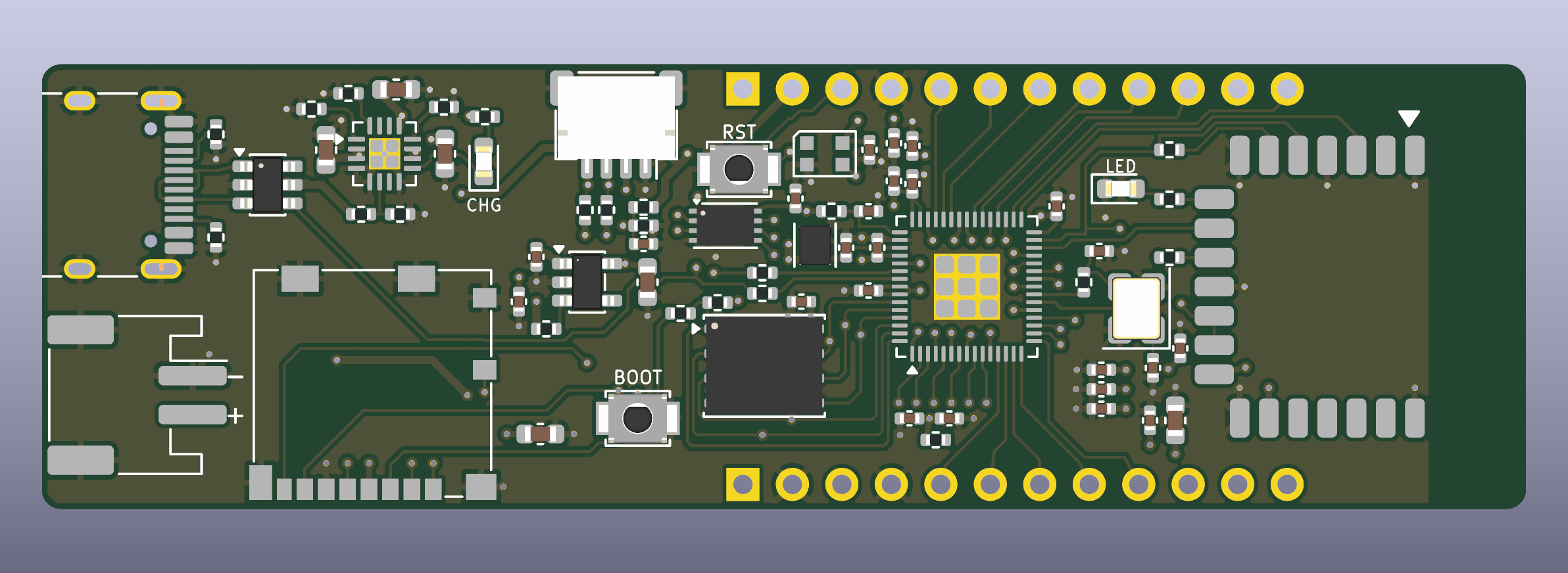
Status: designed, not built. ERC is clean; DRC is clean (0 errors, 0 unconnected, schematic parity OK, one harmless "dangling via" warning). Nothing here has been verified on hardware — read "What a reviewer should check" before ordering.
Where things are
| Path | What |
|---|---|
boards/rp2350-devboard/ |
KiCad project: .kicad_pro, .kicad_sch, .kicad_pcb, project symbol lib, custom DRC rule |
fab/rp2350-devboard-gerbers.zip |
Gerbers (RS-274X, 4 copper layers) + Excellon drill files — upload this to PCBWay |
fab/gerbers/ |
The same files unzipped |
fab/assembly/rp2350-devboard-bom.csv |
BOM in PCBWay's column layout (36 lines, 71 parts, all SMD) |
fab/assembly/rp2350-devboard-centroid.csv |
Pick-and-place file (origin = bottom-left board corner, mm) |
fab/assembly/rp2350-devboard-assembly-top.pdf |
Assembly drawing with reference designators and notes |
fab/docs/ |
Schematic PDF, fab drawing, IPC-D-356 netlist, STEP model, renders |
tools/ |
Generator scripts. tools/design.py is the single source for parts, nets and placement |
The files were made with Backplane KiCad 10.99 (newer file format than stock KiCad 10.0).
PCBWay order settings
- 4 layers, 76.2 x 22.86 mm, 1.6 mm FR-4, 1 oz outer / 0.5 oz inner is fine
- Min track/space 0.15 / 0.10 mm (the 0.10 mm spacing occurs only where VREG_LX passes between two 0402 pads; everything else is ≥ 0.15 mm), min hole 0.3 mm, via 0.6 / 0.3 mm
- Finish: ENIG (0.4 mm pitch QFN-60), any solder-mask colour, vias tented
- Assembly: top side only, turnkey. Stencil top only
- Not populated on purpose: the two 1x12 2.54 mm header rows (J5, J6) and the three bottom-side SWD test pads (TP1–TP3). They are bare holes/pads and are excluded from BOM and centroid
- L1 is polarised: the dot on the Abracon inductor goes to pad 1 (+1V1 net, the pad towards the bottom board edge). This is in the BOM notes and on the assembly drawing
What is on the board
| Function | Part | Notes |
|---|---|---|
| MCU | RP2350A (QFN-60, A4 stepping) | on-chip 1.1 V SMPS with the Abracon AOTA-B201610S3R3-101-T inductor, 12 MHz ABM8-272-T3 crystal |
| Flash | W25Q128JVPIQ, 16 MB | QSPI CS0 |
| PSRAM | APS6404L-3SQR-ZR, 8 MB | QSPI CS1 on GPIO0, 10 k pull-up |
| USB | USB-C (HRO TYPE-C-31-M-12) | 5.1 k CC resistors, USBLC6-2SC6 ESD, 27 Ω series resistors |
| Charger | BQ24074 | power path, ~300 mA charge, 500 mA USB input limit, orange CHG LED |
| 3.3 V | TLV75733P 1 A LDO | fed from the charger's system output; EN on a header pin |
| Battery monitor | 200 k / 200 k divider + 100 nF | VBAT/2 on GPIO29 (ADC3) |
| Wi-Fi / BLE | Raspberry Pi Radio Module 2 (CYW43439) | wired like Pico 2 W, user LED on the module's GPIO0 |
| microSD | Molex 104031-0811 | 4-bit SDIO or SPI0, card-detect on GPIO1 |
| Qwiic / STEMMA QT | JST SM04B-SRSS-TB | I2C0 on GPIO24/25 with 2.2 k pull-ups |
| RGB LED | WS2812B-2020 (V6) | GPIO23, powered from 3.3 V |
| Buttons | 2 x Omron B3U-1000P | BOOT (QSPI_SS through 1 k) and RST (RUN) |
Pin map
| GPIO | Use | GPIO | Use |
|---|---|---|---|
| 0 | PSRAM CS (XIP_CS1) | 16 | RM2 WL_ON (also BT_ON) |
| 1 | SD card detect (low = card in) | 17 | RM2 CS |
| 2 | SD CLK (SPI0 SCK) | 18 | RM2 data (DIN direct, DOUT via 470 Ω, IRQ via 10 k) |
| 3 | SD CMD (SPI0 TX) | 19 | RM2 clock |
| 4 | SD D0 (SPI0 RX) | 20–22 | header |
| 5, 6 | SD D1, D2 | 23 | RGB LED data |
| 7 | SD D3 / CS | 24, 25 | SDA, SCL (header + Qwiic) |
| 8–15 | header | 26–28 | header (ADC0–2) |
| 29 | battery voltage / 2 (ADC3) |
Headers (0.8" row spacing, breadboard-friendly, pin 1 nearest the USB end):
- Top row: VBUS, VBAT, EN, GND, GP28, GP27, GP26, SCL (GP25), SDA (GP24), GP22, GP21, GP20
- Bottom row: 3V3, GND, VSYS, GND, GP8, GP9, GP10, GP11, GP12, GP13, GP14, GP15
Pin names are printed on the bottom silkscreen. SWCLK, SWDIO and GND are test pads on the bottom.
For the Pico SDK, build for a Pico 2 W-style board with CYW43_PIN_WL_REG_ON=16, CYW43_PIN_WL_CS=17,
CYW43_PIN_WL_DATA_OUT/IN/HOST_WAKE=18, CYW43_PIN_WL_CLOCK=19.
Key decisions
- RP2350A, not B. 30 GPIO is enough: 14 are used on the board and 16 go to the headers.
- Raspberry Pi RM2 for the radio rather than an ESP32 co-processor. It works with the stock Pico SDK / MicroPython CYW43 driver, carries its own antenna and modular certification, and needs only four GPIOs. The antenna end sits at the board edge with a 5 mm copper-free strip on all layers.
- BQ24074 + LDO. A true power path lets the board run from USB with no battery or a flat one. I chose an LDO over a buck-boost to keep the layout simple; the cost is that 3.3 V sags once the cell drops below about 3.5 V (the RM2 wants ≥ 3.0 V, ≥ 3.2 V for full RF performance).
- Charge current ~300 mA (R7 = 3.0 k; I = 890 / R7). Suits cells of 300 mAh and up; change R7 for other cells.
- Regulator layout copies the Raspberry Pi reference: VREG_LX runs between the pads of the input and output capacitors to the inductor, with one shared capacitor for pins 53/54. That is where the 0.10 mm spacing comes from (a custom DRC rule allows it for that net only).
- All parts on top. This made the board long (76 mm). Putting the microSD socket on the back would save about 14 mm at the price of double-sided assembly.
- How the files were made. Schematic and board are generated from
tools/design.py. The RP2350 fan-out, regulator, QSPI, SD bus and other critical routes are explicit coordinates in that file; the remaining ~60 connections were finished by a small grid router (tools/maze.py) and checked with KiCad's DRC. The routing is electrically clean but not hand-polished.
What a reviewer should check
- Battery polarity. J2 pin 2 (marked
+, the pad nearer the bottom edge) is positive. I could not confirm this matches the common Adafruit/SparkFun JST-PH wiring. Check your cell before plugging in — there is no reverse-polarity protection. - microSD card-detect pins. I wired socket pad 9 to GPIO1 and pad 10 to GND, assuming the switch sits between those two pads. If Molex's drawing says otherwise, card detect will read wrong; the card itself still works.
- RM2 footprint is KiCad's library footprint
RF_Module:RMC20452T; I checked its pad positions against the RM2 datasheet drawing, not against a physical module. - Three signals use short tracks on In2 (the 3.3 V plane): QSPI SD1 and SD2 to the PSRAM, PSRAM CS, and RUN to the reset button. They were the only way to cross the SD bus and radio lines with single-sided assembly. They cut narrow slots in the plane; the GND plane on In1 is unbroken.
- Decoupling is a compromise. Most mid-side RP2350 supply pins drop to the planes through vias inside the pad ring, with their 100 nF capacitors 3–6 mm away. Raspberry Pi's own minimal design makes a similar trade, but this is the first thing I would probe on a prototype (1.1 V ripple under Wi-Fi load).
- Things left out to keep the layout routable:
- no external pull-ups on the SD lines (use the RP2350's internal ones);
- no external pull-up on RUN (internal only) and RUN is not on a header pin;
- the RM2's GPIO2 is not wired to VBUS sense as on a Pico W;
- no fiducials or mounting holes.
- Battery sense leakage. The divider draws about 10 µA from the cell all the time, and GPIO29 is not fail-safe: with 3.3 V switched off through EN a few µA flow into the pin.
- Power track widths are 0.25–0.4 mm for VBUS/VBAT/VSYS. That is adequate for the 500 mA input limit but not generous.
- BOM part numbers. ICs, connectors, LEDs and switches were checked against LCSC stock on 2026-11-09 (the RM2 had only 51 pieces there; PCBWay may source it elsewhere). The Yageo/Samsung passive part numbers were written from the manufacturers' naming scheme and not looked up — any equivalent 0402/0603 part of the same value and rating is fine.
- The USB pair is routed for full-speed only (no impedance control), which is all the RP2350 supports.
Regenerating
tools/build_all.sh            # schematic, netlist check, pours, DRC, fab outputs (keeps the routing)
tools/build_all.sh --reroute  # also throws the routing away and routes again (about 2 minutes)