Rank 3 of 7 in RP2350 dev board
Opus 5.5 in Backplane
Anthropic's Opus 5.5 on medium reasoning, in Backplane hub driving Claude Code.
69.9 of 100
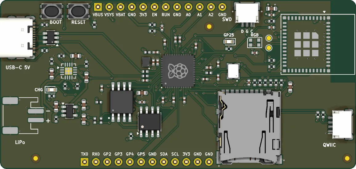
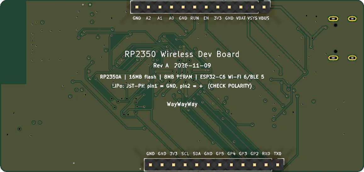
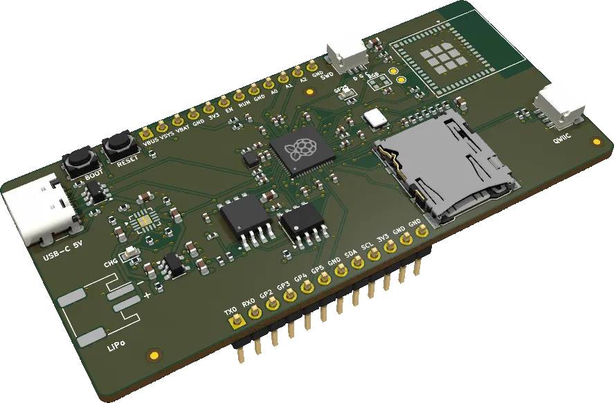
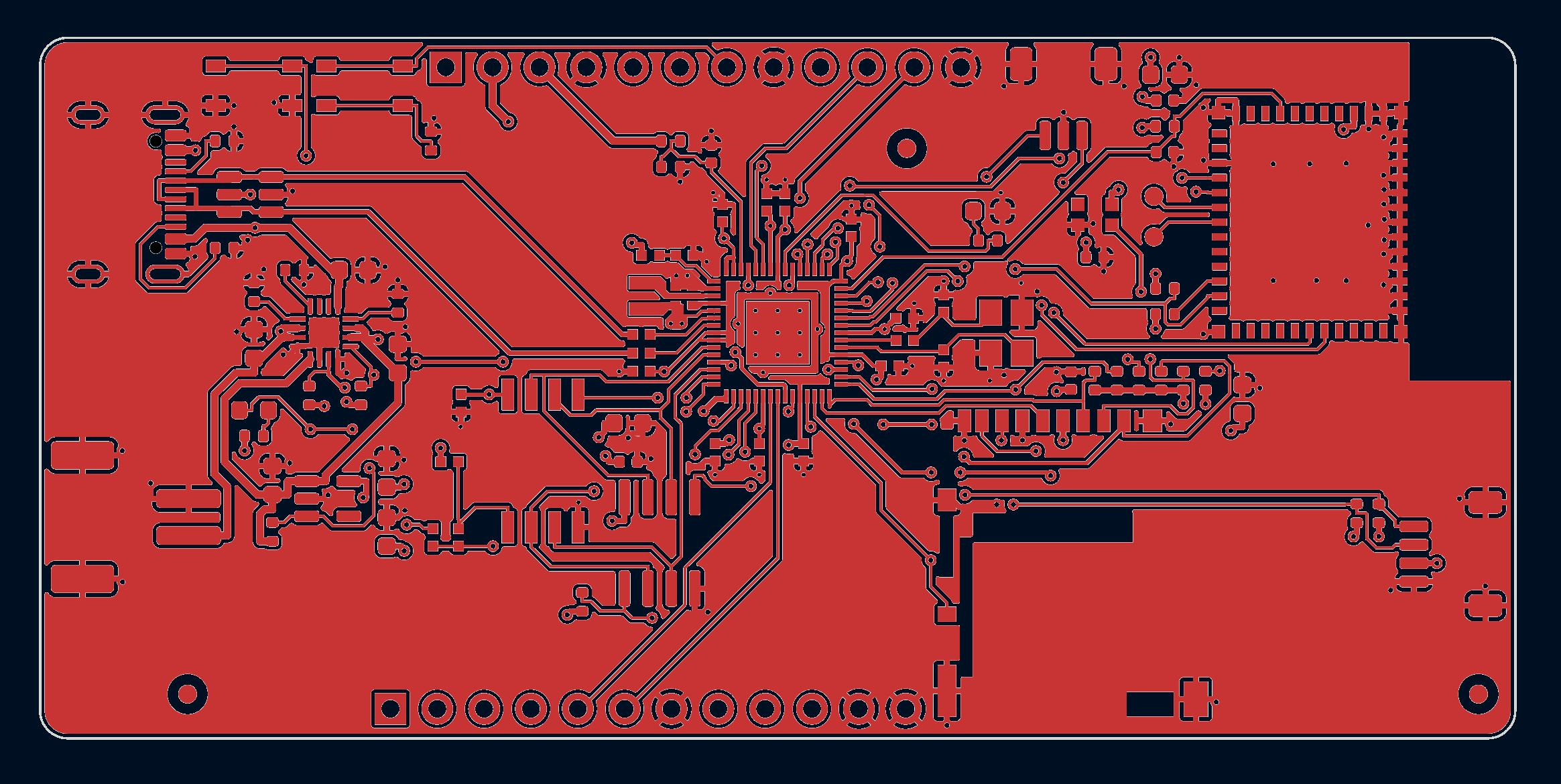
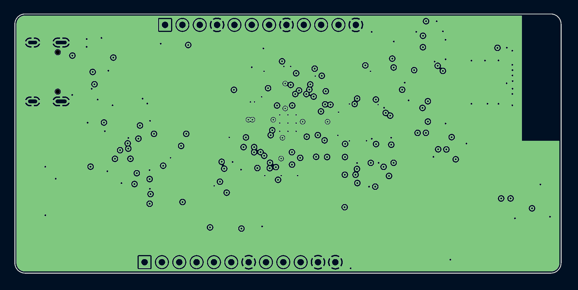
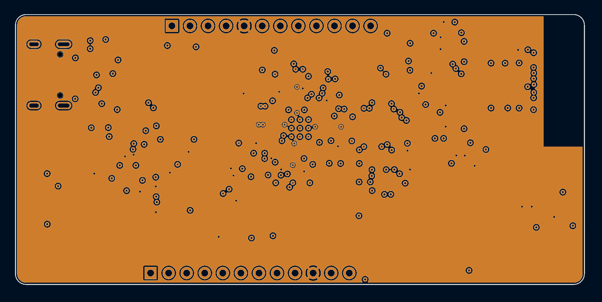
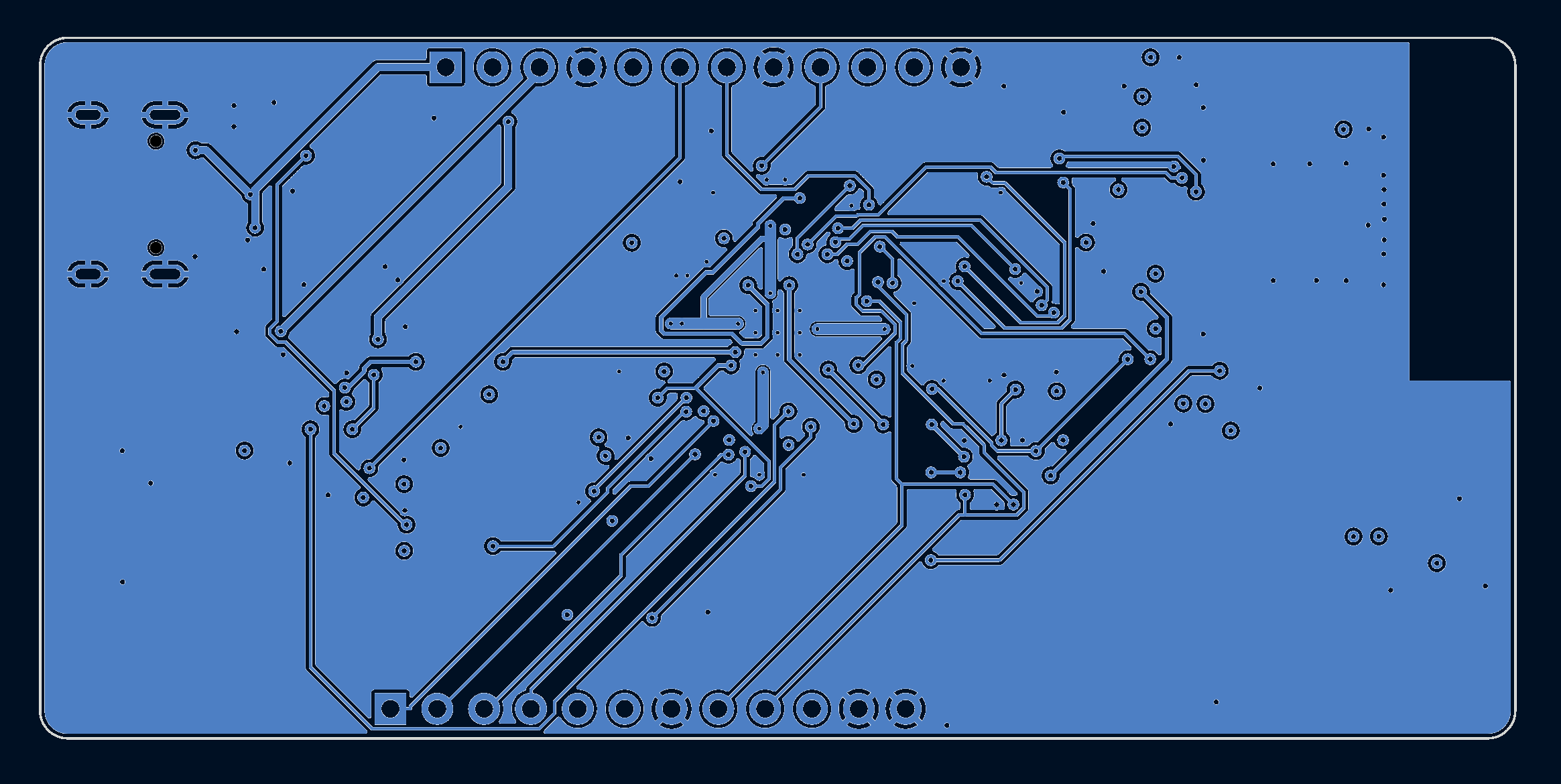
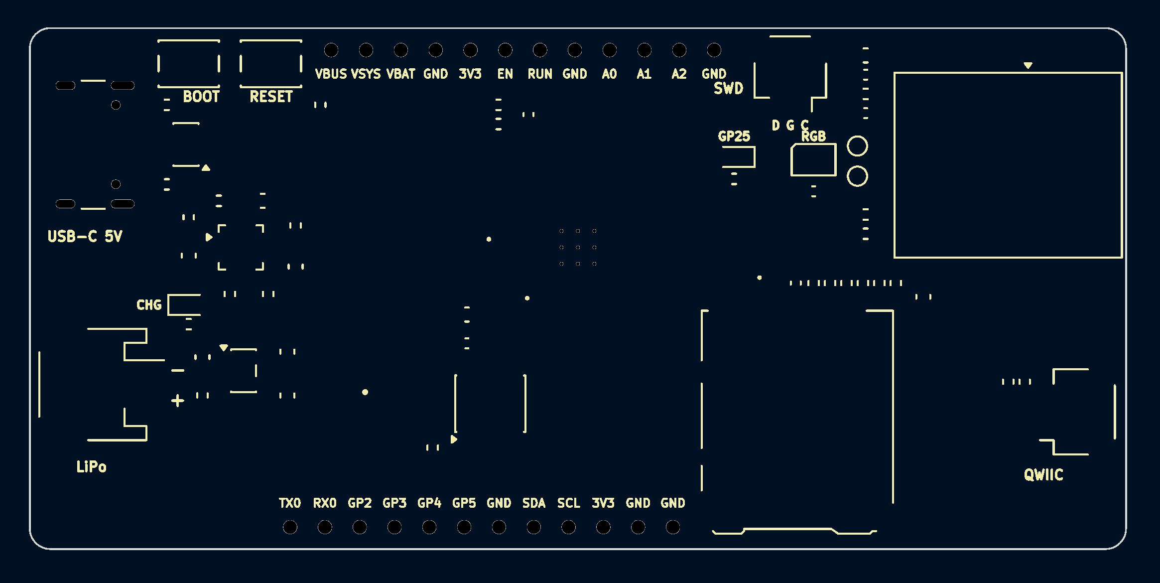
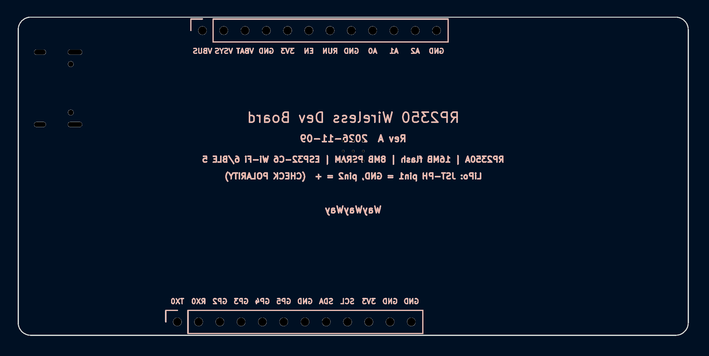
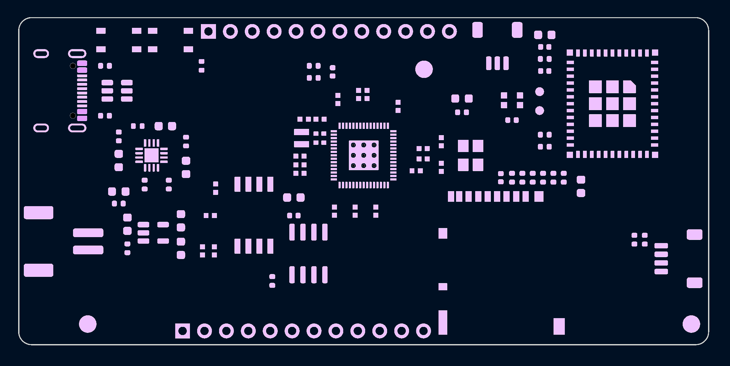
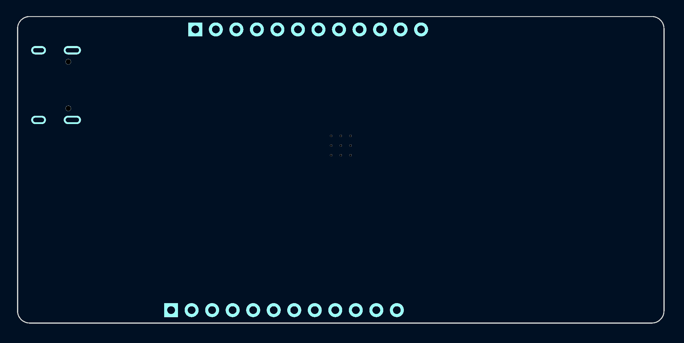
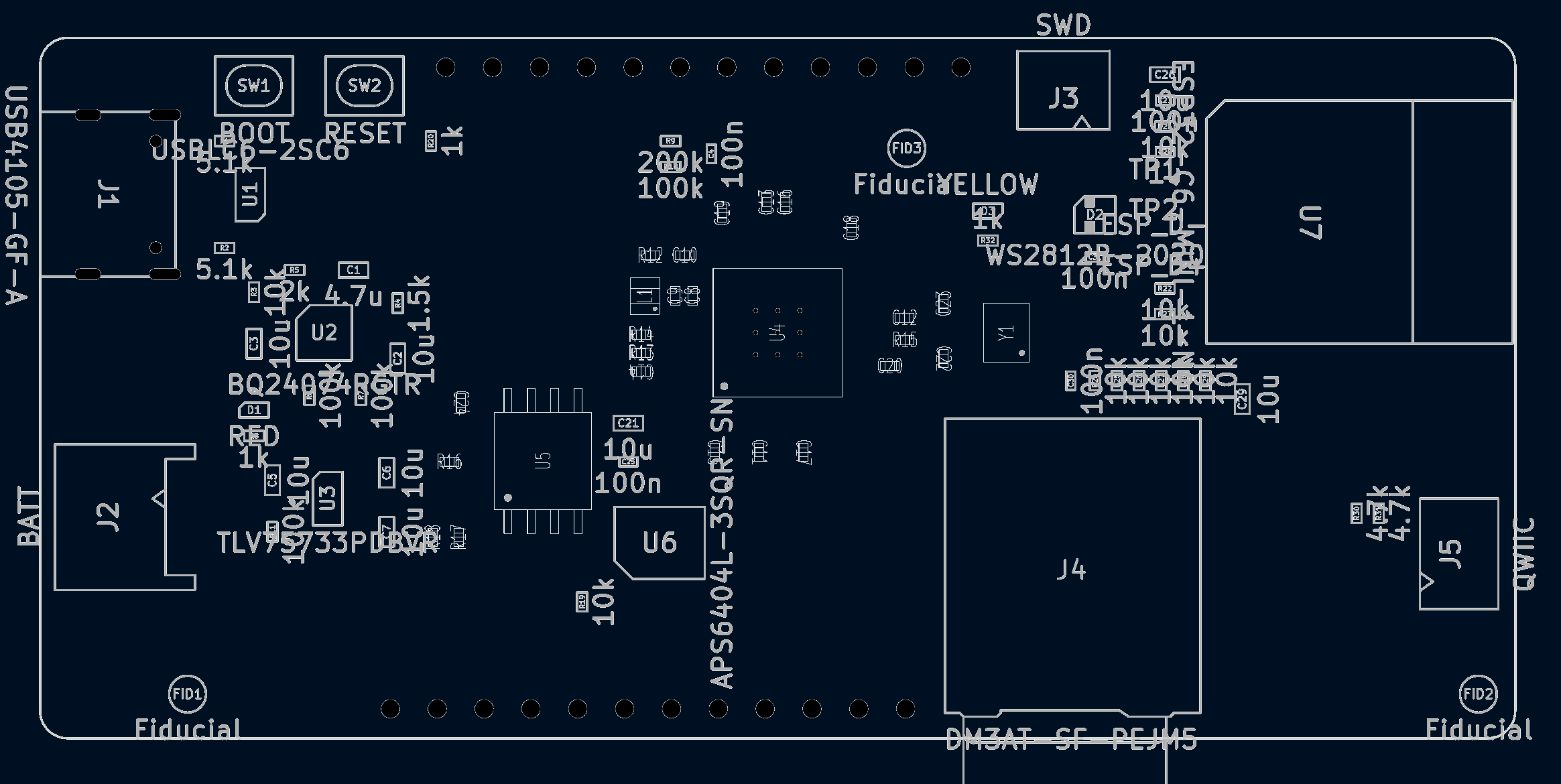
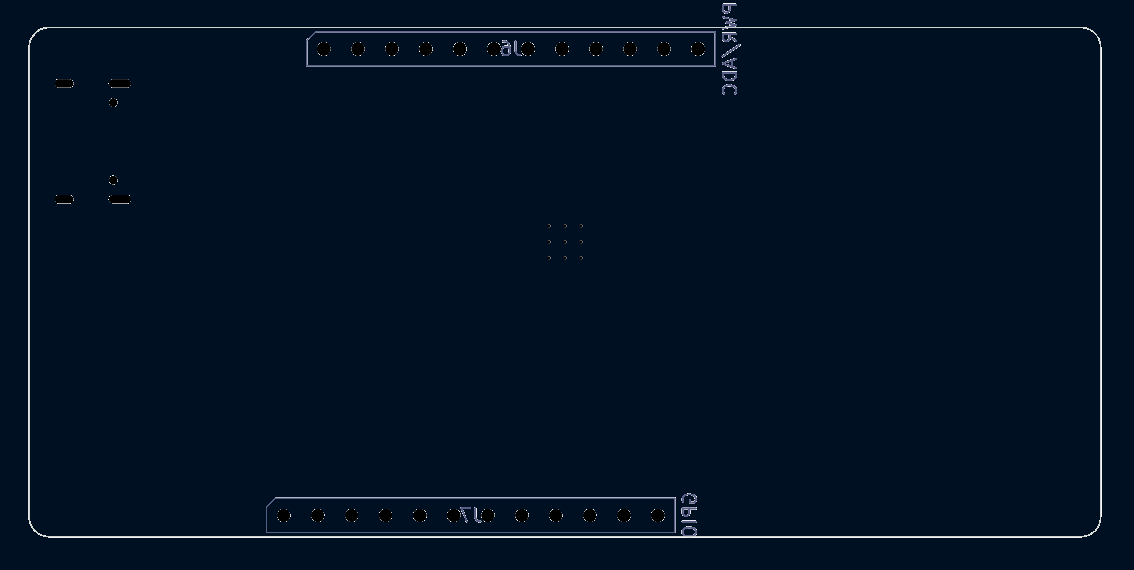
Rendered by kicad-cli with the run's own KiCad version. Dimensions in mm. The layers are the plots the AI judge saw, seen from the top, with their white background made dark. Click one to open it at full size.
- AI cost
- $56.77
- Time
- 2 h 50 min
- Tokens, incl. cache reads
- 124.9M
- 1 board
- $185.16
- 5 boards, per board
- $51.57
- Board size
- 80 × 38 mm
- Machine
- EC2 Ubuntu (c7i.2xlarge)
- backplane
- backplane-hub 0.15.0
- claudeCode
- 2.1.321 (Claude Code)
- codex
- codex-cli 0.167.0
- kicad
- 10.99.0-bp.4 (5dbc22d292704d02b609d5b7a0edc971f1b7f08b)
Score
Design review17 of 20
- Layout10 of 101 minus 0.1 per minor and 0.2 per major layout finding, down to 0
- Routing7 of 10the same, for routing findings
Circuit checks17.8 of 20
- Decoupling5 of 5RP2350 power pins with a capacitor within 3.2 mm
- USB protection5 of 50.5 for an ESD part on D+ and D−, plus 0.25 for each line with a series resistor
- Antenna keepout5 of 51 when there are keepouts and no copper is in them
- Battery drain2.8 of 51 at 5 µA or less drawn by unswitched battery dividers, falling linearly to 0 at 25 µA
Layout checks15.4 of 30
- Thermal pads5 of 10mean over the exposed pads of their vias over the number needed, 0 for a pad with no plane on another layer
- Grounding7.1 of 10USB, QSPI and microSD track length over a ground plane on the next layer
- Silkscreen0.4 of 5texts at least 0.8 mm high
- Board size3 of 51 at the Feather RP2350's 50.8 × 22.8 mm area or less, falling linearly to 0 at 5 times that area
Orderable10 of 20
- Fab notes0 of 51 when every fab option in the notes can be ordered from PCBWay
- Board0 of 51 when the board needs no rework
- BOM lines10 of 101 minus 0.2 for each BOM line that needs a fix, down to 0
Parts data9.8 of 10
- 3D models4.8 of 5parts with a 3D model
- Supplier part numbers5 of 5BOM lines with a valid number from at least one supplier
| The five groups | 70 |
|---|---|
| Every gate passed, so no penalty | 0 |
| Score | 69.9 of 100 |
Gates
A board that fails a gate loses 20 points. The gates are the three checks below, every prompt feature, and any fatal review finding.
| Check | Result | What the check found |
|---|---|---|
| Crystal and load capacitors | Pass | Y1 ABM8-272-T3 (CL 10 pF) between XIN and XOUT via R15 1k; load caps XIN: C22 15p; XOSC_R: C23 15p; needs 10.5–17.5 pF per side for 3 pF stray |
| BOOTSEL and RUN buttons | Pass | QSPI_SS (QSPI_SS) → R18 → SW1 → GND; RUN (RUN) → SW2 → R20 → GND |
| Charger power path | Pass | U2 BQ24074RGTR: U2 IN (VBUS) is on J1 VBUS; BAT (VBAT) goes to J2; U3 TLV75733PDBVR makes +3V3 from OUT (VSYS) |
Prompt features
- Found RP2350 U4
- Found QSPI flash U5
- Found PSRAM U6
- Found USB-C J1
- Found Wi-Fi and BLE U7
- Found microSD J4
- Found Qwiic J5
- Found RGB LED D2
- Found Power-path charger U2
- Found Battery monitoring R9
Design review 17 of 20
Opus 5.5 reviewed an anonymous copy of the board and listed 3 findings. Layout and routing each start at 10 points.
Minor
Routing
The charger output and the battery path are 0.4 mm tracks on 35 um outer copper. At 1.5 A, IPC-2221 gives about a 16 C rise. A 10 C rise needs about 0.53 mm, so these tracks should be at least 0.6 mm. The VSYS feed to the header also drops through a single 0.3 mm via.
Evidence
VSYS on F.Cu at 0.4 mm: U2 pads 10/11 (116.84, 116.25/115.75) -> C2 pad 1 (119.40, 118.18) -> segment (119.40, 119.80)-(115.48, 123.72) -> U3 pad 1 (114.46, 124.05). VBAT on F.Cu at 0.4 mm: J2 pad 2 (108.05, 127.00) -> (110.15, 127.00) -> (109.46, 123.67)-(109.46, 119.33) -> C3 pad 1 (111.60, 117.38) -> U2 pads 2/3 (113.96, 115.75/116.25). The stackup gives F.Cu and B.Cu 0.035 mm thick. VSYS reaches J6 pad 2 only through the 0.6/0.3 mm via at (118.32, 116.36) and a 0.4 mm B.Cu track.
Adding the PSRAM made the router put 2 vias on each path of QSPI_SD0, QSPI_SD1 and QSPI_SS, and one of them sits under the RP2350 body. The Raspberry Pi minimal reference that the flash placement copies routes these nets with no vias. The PSRAM branches of SD0, SD1 and SD3 also run 1.7 to 2.3 times their straight distance.
Evidence
QSPI_SD0 vias at (137.47, 117.77), inside the U4 outline between pad 57 and the EP, plus (133.49, 119.53) and (138.55, 124.32). Its PSRAM branch goes out on B.Cu to (139.53, 122.98)-(139.53, 123.92) and comes back on F.Cu (138.55, 124.32)-(136.40, 124.32) to U6 pad 5: 12.96 mm routed vs 7.40 mm straight. QSPI_SD1 vias at (135.05, 119.53) and (130.04, 124.60). It daisy-chains through U5 pad 2 to U6 pad 2: 22.8 mm vs 12.0 mm. QSPI_SS vias at (135.04, 120.28) and (124.56, 127.58). QSPI_SD3 from U4 pad 55 to U6 pad 7: 20.4 mm vs 8.9 mm. In RPI-RP2350A-MINIMAL_R4-S1, QSPI_SD0, SD1 and SS have 0 vias.
SD_D3 takes a 39 mm detour on B.Cu that loops up past the crystal, while the direct distance is 15 mm and the other SD lines are 13 to 20 mm. SD_D2 changes layers 4 times and leaves a 10 mm stub past the socket pad to reach its pull-up.
Evidence
SD_D3: U4 pad 19 (143.45, 117.60) -> via (144.37, 117.76) -> B.Cu north to (144.44, 111.65) -> (145.83, 110.80) -> (151.08, 116.05) -> (158.81, 116.05), which passes under Y1 -> via (160.20, 117.43) -> J4 pad 2 (157.68, 120.78). That is 38.9 mm routed vs 14.6 mm straight. SD_D2 vias at (142.75, 118.00) under U4, (145.73, 120.98), (148.35, 120.98) and (150.10, 122.73). Past J4 pad 1 (158.78, 120.78), SD_D2 runs on through (162.21, 121.60), (164.50, 117.80) and (160.86, 117.54) to R27 pad 2.
Opus 5.5's notes
I wrote review.json with three findings, all minor. I found nothing fatal and no layout problems: I'd expect this board to work as built.
Upgrade
I upgraded all five schematics and the board in place with kicad-cli sch upgrade and kicad-cli pcb upgrade:
- Schematics: from format 20260306 (KiCad 10.0) to 20261106 (10.99).
- Board: from 20260901 to 20261031.
Nothing else in the design changed. DRC on the upgraded board finds 0 unconnected items and 3 connection-width warnings in the copied RPi regulator copper.
Findings
| # | Area | Nets | Problem |
|---|---|---|---|
| 1 | routing | VSYS, VBAT | The charger output and battery path are 0.4 mm tracks on 35 µm copper. At 1.5 A that is about a 16 °C rise by IPC-2221; a 10 °C rise needs about 0.53 mm. VSYS reaches the header through a single 0.3 mm via. |
| 2 | routing | QSPI_SD0, SD1, SS | Each path has 2 vias, and one sits under the RP2350 body at (137.47, 117.77). The Raspberry Pi reference uses none. The PSRAM branches run 1.7 to 2.3 times their straight distance. |
| 3 | routing | SD_D3, SD_D2 | SD_D3 is 38.9 mm long against 14.6 mm straight, looping on B.Cu under the crystal. SD_D2 has 4 vias and a 10 mm stub to its pull-up. |
What I checked and left out
- Matches the Raspberry Pi reference: I downloaded the Raspberry Pi RP2350A minimal reference board and compared it pad by pad. The RP2350 footprint, the regulator inductor and its orientation, the crystal and the flash sit exactly where the reference puts them, rotated 90°. That is why I didn't report the flash at about 10 mm or the crystal at about 9 mm from their pins.
- Pinouts on the right nets: I checked these against datasheets or standard pinouts:
- BQ24074 charger: EN2 high and EN1 low select the ILIM resistor, and TMR and ITERM left open select the defaults.
- ESP32-C6-MINI-1 module: pins and land pattern, and it isn't mirrored.
- Flash, PSRAM, microSD, LDO, ESD array, RGB LED, LEDs, SWD and Qwiic pinouts.
- Connectors and antenna face out: the USB-C edge line is at x = 100. The JST, Qwiic, SWD and microSD openings face their edges, and the antenna ends at x = 179.85 with nothing in front of it.
- Not reported, because your automated checks cover it: USB D+ and D− run about 5 mm apart over roughly 10 mm, so they aren't a coupled pair. That only matters for impedance, and full-speed USB tolerates it.
I put my scratch files in .scratch/ inside the folder and deleted them at the end, along with the board.kicad_prl that kicad-cli created. Two slips: I briefly copied the project to /tmp before moving the copy into the folder, and I wrote one scratch script with a shell heredoc instead of apply_patch.
Circuit checks 17.8 of 20
Decoupling
5 of 514 of 14 RP2350 power pins have a capacitor within 3.2 mm.
| Pin | Pad | Net | Nearest capacitor | Distance |
|---|---|---|---|---|
| IOVDD | 1 | +3V3 | C15 | 2.63 mm |
| DVDD | 6 | +1V1 | C11 | 2.56 mm |
| IOVDD | 11 | +3V3 | C17 | 2.57 mm |
| IOVDD | 20 | +3V3 | C20 | 2.24 mm |
| DVDD | 23 | +1V1 | C12 | 3.06 mm |
| IOVDD | 30 | +3V3 | C18 | 2.47 mm |
| IOVDD | 38 | +3V3 | C16 | 3.19 mm |
| DVDD | 39 | +1V1 | C13 | 3.16 mm |
| ADC_AVDD | 44 | +3V3 | C8 | 2.4 mm |
| IOVDD | 45 | +3V3 | C8 | 2.04 mm |
| VREG_AVDD | 46 | VREG_AVDD | C10 | 1.8 mm |
| VREG_VIN | 49 | +3V3 | C8 | 1.17 mm |
| USB_OTP_VDD | 53 | +3V3 | C8 | 1.88 mm |
| QSPI_IOVDD | 54 | +3V3 | C8 | 2.21 mm |
USB protection
5 of 5- ESD parts on D+ and D−
- U1
- D+ nets, connector to RP2350
- USB_DP → USB_DP_MCU series resistor
- D− nets, connector to RP2350
- USB_DM → USB_DM_MCU series resistor
Differential pair, not scored
- D+ and D− length
- 38.02 mm and 38.29 mm
- Mismatch
- 0.27 mm
- Vias
- 0
- Longest coupled stretch
- 11.78 mm on F.Cu, 0.25 mm wide, 1.25 mm gap
- Differential impedance
- 120.9 Ω
Antenna keepout
5 of 52 keepouts cover the Wi-Fi module U7.
| Keepout | Layers | Copper inside |
|---|---|---|
| U7 footprint, ANT_KEEPOUT | F.Cu, B.Cu, In1.Cu, In2.Cu | none |
| Board, ANTENNA_KEEPOUT_BOARD | F.Cu, B.Cu, In1.Cu, In2.Cu | none |
Battery drain
2.8 of 5Unswitched dividers draw 14 µA from a full battery, even when the board is off.
| Divider | Buffered by | Switched by | At 4.2 V |
|---|---|---|---|
| R9 200k / R10 100k | none | none | 14 µA |
Layout checks 15.4 of 30
Thermal pads
5 of 10| Exposed pad | Net | Vias | Needed | Plane on another layer |
|---|---|---|---|---|
| U4 | GND | 9 | 9 | yes |
| U2 | GND | 0 | 5 | yes |
Grounding
7.1 of 10| Bus | Over ground | Track length | Share |
|---|---|---|---|
| USB | 76.3 mm | 76.3 mm | 100% |
| QSPI | 95.3 mm | 132.1 mm | 72.1% |
| microSD | 106.5 mm | 185.3 mm | 57.5% |
| All three | 278.1 mm | 393.7 mm | 70.6% |
Silkscreen
0.4 of 560 of 65 texts are below PCBWay's 0.8 mm minimum. The smallest is 0.6 mm.
Board size
3 of 580 × 38 mm, 3040 mm². The Feather RP2350 is 50.8 × 22.8 mm.
Orderable 10 of 20
| 1 board | 5 boards | |
|---|---|---|
| PCBs | $62.04 | $62.04 |
| Assembly | $88.00 | $89.26 |
| Components | $35.12 | $106.53 |
| Total | $185.16 | $257.83 |
| Per board | $185.16 | $51.57 |
PCBWay's instant quote for the options in the fab notes, without shipping. PCBWay makes at least 5 PCBs, so 1 board is 5 PCBs with 1 assembled. Parts are at distributor list prices. The prices include the fixes below.
Fixes made to price the order
| Area | Parts | Problem | Fix |
|---|---|---|---|
| Fab notes | The fab notes ask for 0.5 oz inner copper, which PCBWay does not offer | Quoted 1 oz inner copper |
Fab notes
0 of 5- The fab notes ask for 0.5 oz inner copper, which PCBWay does not offer
Board
0 of 5- 3 DRC errors
BOM lines
10 of 100 of 38 BOM lines need a fix.
Parts data 9.8 of 10
3D models
4.8 of 54 parts have no 3D model the run's KiCad can load: D2, J2, U2, U7.
Supplier part numbers
5 of 538 of 38 BOM lines have a valid supplier part number.
LCSC 100%, Digi-Key 0%, Mouser 0%
Stock
100% of 38 BOM lines are stocked for 5 boards at LCSC, JLCPCB or Digi-Key.
DRC and ERC
| Errors | Warnings | Unconnected | |
|---|---|---|---|
| DRC | 3 | 0 | 0 |
| ERC | 0 | 0 |
DRC by type: connection_width 3.
Files
The agent's README
RP2350 Wireless Dev Board (Rev A)
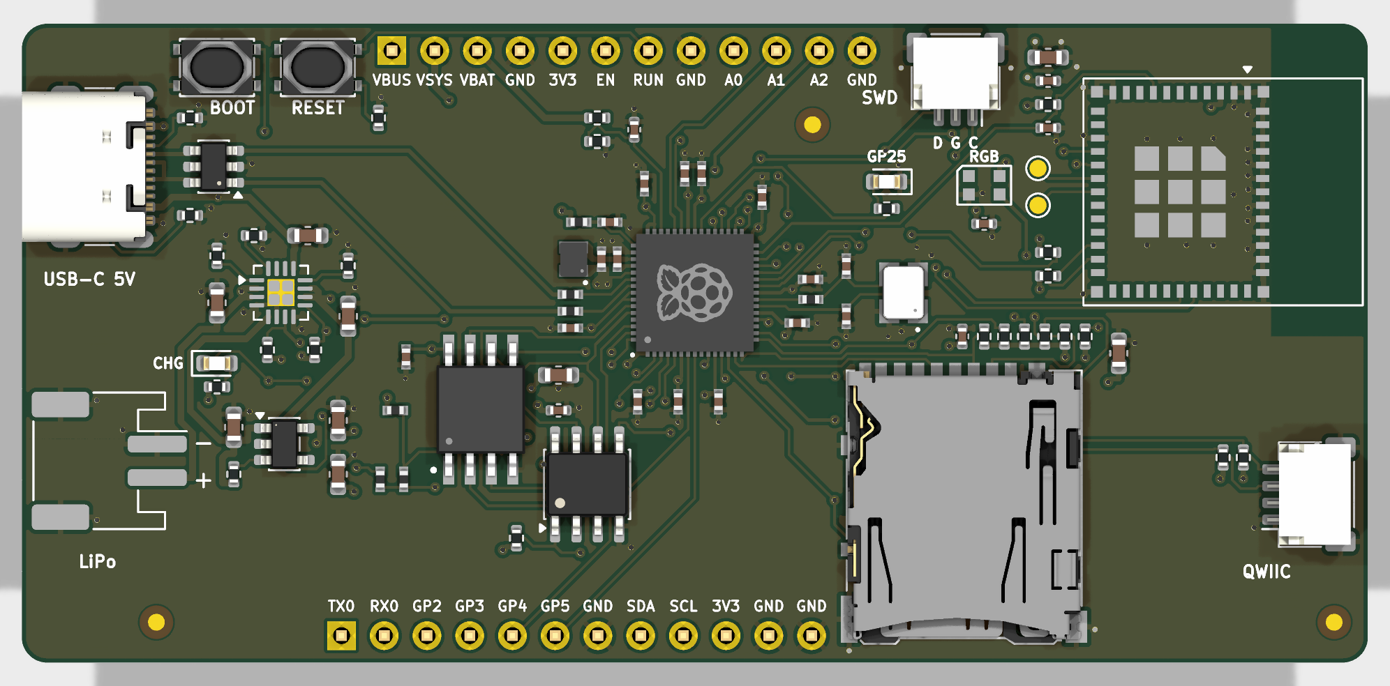
An 80 × 38 mm, 4-layer RP2350 development board designed for turnkey manufacture and assembly by PCBWay (every part on the BOM is placed by PCBWay; all SMD parts are on the top side, the two pin headers are the only through-hole parts).
| Feature | Implementation |
|---|---|
| MCU | Raspberry Pi RP2350A (QFN-60), 150 MHz dual Cortex-M33 / Hazard3 |
| Flash | W25Q128JVSIQ, 16 MB QSPI on QSPI_SS |
| PSRAM | APS6404L-3SQR-SN, 8 MB QSPI PSRAM on XIP_CS1 = GPIO8 |
| USB | USB-C (GCT USB4105-GF-A), USB 2.0 FS device + 5 V input, 5.1 kΩ Rd on CC1/CC2, USBLC6-2SC6 ESD |
| Battery | 1-cell Li-Po on JST-PH 2-pin (pin 1 = GND, pin 2 = +) |
| Charger / power-path | TI BQ24074 (DPPM power-path: USB powers the system and charges the cell, the cell takes over seamlessly) |
| Battery monitor | VBAT / 3 divider on GPIO29 / ADC3 (same scaling as Pico 2), charger ~CHG on GPIO7, ~PGOOD (USB present) on GPIO6 |
| 3.3 V | TLV75733P 1 A LDO from VSYS, enable on header (EN) |
| Wi-Fi + Bluetooth LE | ESP32-C6-MINI-1-N4 module (Wi-Fi 6 2.4 GHz, BLE 5, 802.15.4), PCB antenna at the board edge, UART link with RTS/CTS to RP2350 |
| microSD | Hirose DM3AT-SF-PEJM5 push-push socket with card detect, wired for 4-bit SDIO (PIO) and SPI |
| Qwiic / STEMMA QT | JST-SH 4-pin (SM04B-SRSS-TB), I²C0 on GPIO16/17, 4.7 kΩ pull-ups, 3.3 V |
| RGB LED | WS2812B-2020 addressable LED on GPIO24 |
| Other | BOOT and RESET buttons, user LED (GPIO25), charge LED, SWD on JST-SH 3-pin (Raspberry Pi Debug Probe pinout), 2 × 12-pin 2.54 mm headers |
Repository layout
boards/rp2350-dev/      KiCad 10 project (schematic: 5 sheets, 4-layer PCB, project footprint library)
  rp2350-dev.kicad_pro / .kicad_sch / .kicad_pcb
  power.kicad_sch mcu.kicad_sch wireless.kicad_sch io.kicad_sch
  lib/RP2350_Dev.pretty  project footprints (see "Footprints")
fab/                    everything PCBWay needs (see "Ordering from PCBWay")
scripts/                the generators used to build the design (design.py is the single source of truth)
third_party/            Raspberry Pi RP2350A minimal design (MIT) used as the core reference
Footprints
Standard KiCad library footprints are used except for boards/rp2350-dev/lib/RP2350_Dev.pretty:
| Footprint | Source |
|---|---|
RP2350A_QFN60_RPi |
RPi reference RP2350A footprint, with its 9 EP vias and embedded 3D model |
L_Abracon_AOTA-B201610 |
RPi reference footprint for the polarity-marked 3.3 µH inductor |
C_0402_RPi, C_0402_RPi_Wide, R_0402_RPi, Crystal_3225_RPi, SOIC-8_5.3mm_RPi |
RPi reference passive/crystal/flash footprints (keep the copied tracks landing exactly on the pads) |
ESP32-C6-MINI-1_BoardEdge |
KiCad RF_Module:ESP32-C6-MINI-1 with the courtyard cut to the module outline and an all-layer copper keepout under the antenna. The stock footprint draws Espressif's ideal 43 mm-wide antenna clearance as its courtyard. |
scripts/extract_rpi.py and scripts/make_esp_fp.py regenerate them.
GPIO map
| GPIO | Function | GPIO | Function |
|---|---|---|---|
| 0 | UART0 TX (header J7) | 16 | I²C0 SDA (Qwiic + header) |
| 1 | UART0 RX (header J7) | 17 | I²C0 SCL (Qwiic + header) |
| 2–5 | header J7 | 18 | ESP32-C6 EN (drive low = reset; use open-drain style) |
| 6 | BQ24074 ~PGOOD (low = USB power present) |
19 | ESP32-C6 IO9 boot strap (low at reset = ROM download) |
| 7 | BQ24074 ~CHG (low = charging) |
20 | UART1 TX → ESP RXD0 |
| 8 | PSRAM CS (XIP_CS1) | 21 | UART1 RX ← ESP TXD0 |
| 9 | microSD card detect (switch to GND, 10 k pull-up) | 22 | UART1 CTS ← ESP IO6 (RTS) |
| 10 | SD CLK (SPI1 SCK) | 23 | UART1 RTS → ESP IO7 (CTS) |
| 11 | SD CMD (SPI1 MOSI) | 24 | WS2812B data |
| 12–15 | SD DAT0–DAT3 (DAT0 = SPI1 MISO, DAT3 = CS) | 25 | user LED (yellow) |
| 26–28 | ADC0–2 (header J6) | ||
| 29 | VBAT / 3 (ADC3) |
Headers (pin 1 at the left, looking at the top side):
- J6 (top edge): VBUS, VSYS, VBAT, GND, 3V3, EN, RUN, GND, A0/GP26, A1/GP27, A2/GP28, GND
- J7 (bottom edge): GP0/TX, GP1/RX, GP2, GP3, GP4, GP5, GND, SDA/GP16, SCL/GP17, 3V3, GND, GND
Key design decisions
- RP2350 core copied from the Raspberry Pi reference. Raspberry Pi say the RP2350 switching
regulator layout must be copied exactly ("if you choose not to use our example, then you do so at
your own risk"). The RP2350A Minimal design R4 (MIT licence, in
third_party/) was used verbatim for the RP2350A, its footprint with EP vias, the 3.3 µH polarity-marked Abracon AOTA-B201610S3R3-101-T inductor, VREG_VIN/VREG_LX/VREG_AVDD capacitors and 33 Ω filter, all decoupling capacitors, the 12 MHz ABM8-272-T3 crystal (15 pF, 1 kΩ), USB 27 Ω resistors and the QSPI flash with its CS pull-up, 0 Ω link and BOOTSEL resistor.scripts/gen_pcb.pyplaces those parts at the reference positions (rotated 90°) and copies the reference copper — tracks, vias and the VREG_LX / +1V1 / +3V3 / PGND copper areas — for the power, regulator, crystal and USB nets. The QSPI bus was not copied. The reference has only the flash, so the bus was re-routed to reach the PSRAM too. Everything else was placed for this board and routed as described below. - PSRAM on GPIO8, not GPIO0: GPIO8 is a valid XIP_CS1 pin and matches the Adafruit Feather
RP2350, so existing board configurations work (
PICO_RP2350_PSRAM_CS=8). It also keeps GPIO0/1 free for the SDK's default UART0. - ESP32-C6-MINI-1 for Wi-Fi/BLE. The pre-certified module avoids RF matching work and is easy for
PCBWay to source. It runs Espressif's ESP-AT or ESP-Hosted firmware as a co-processor on UART1 with
hardware flow control. The RP2350 drives the module's
ENandIO9strap, so it can put the ESP into ROM download mode and re-flash it over the same UART (esp-serial-flasher).IO8is pulled up, as needed for download mode. The ESP's native USB (IO12/IO13) goes to test pads TP1/TP2 for factory programming. The ESP32-C6 is supplied blank: flash ESP-AT (configured for UART0 TX=IO16 / RX=IO17, RTS=IO6, CTS=IO7) or ESP-Hosted before use, either from the RP2350 or through the USB test pads TP1/TP2. PCBWay also offers pre-programming as a paid option. The antenna sits at the right board edge. A keepout on all copper layers covers the antenna and the strip to the edge. There is no copper under or beside the antenna. - BQ24074 charger with real power-path. It was chosen over an MCP73831 + MOSFET load share for proper DPPM, input OVP to 10.5 V (28 V tolerant), a 1.5 A capability and status pins. Configuration: EN2 = 1, EN1 = 0 → input current limit set by R4 = 1.5 kΩ (≈1.03 A); R5 = 2 kΩ → 445 mA fast-charge (good for ≥ 450 mAh cells; change R5 for other cells: I = 890 / R); TMR open = default safety timers; ITERM open = 10 % termination; TS tied to 10 kΩ (most hobby cells have no NTC; fit an NTC pack and remove R3 if you want temperature qualification). On USB, VSYS is regulated to 4.4 V. On battery, VSYS = VBAT.
- LDO rather than buck-boost for 3.3 V: the TLV75733P (1 A, low dropout) covers ESP32-C6 TX peaks (≈350 mA) plus RP2350, SD and LED. Dissipation at 4.4 V in is ≤ 0.35 W at 300 mA. On battery, 3V3 stays regulated down to VBAT ≈ 3.5 V and then tracks the battery (≈ 3.3 V at 3.5 V cell).
- Battery monitor: a 200 k / 100 k divider (≈14 µA load on the cell, 100 nF filter) gives VBAT/3 on
ADC3 — identical to the Pico 2's VSYS/3 so existing code works (
v = raw * 3.3 / 4096 * 3). - 4-layer stack-up (PCBWay standard 1.6 mm): F.Cu signals + GND pour / In1 solid GND / In2 solid 3.3 V / B.Cu signals + GND pour. This gives every IC a low-impedance return path. The USB pair runs over solid ground.
- microSD wiring supports both modes: D0–D3 sit on consecutive GPIO12–15 for PIO SDIO
(e.g.
no-OS-FatFS-SD-SDIO-SPI-RPi-Pico), and CLK/CMD/D0/D3 line up with SPI1 for SPI mode. - Assembly constraints: all SMD parts are on the top (single-sided reflow). The two headers are THT,
fitted from the bottom (plastic spacer under the board, so the board plugs straight into a
breadboard) and hand/selective soldered. Fiducials: 3 on top. The board text includes
WayWayWay(bottom side), where PCBWay prints its order number.
Reproducing / tools
- KiCad 10.99 (Backplane build of KiCad master). The files use the current master format; to open them in
stock KiCad 10.0, export a copy with
kicad-cli project downgrade --target 10.0. - Python 3 scripts in
scripts/(the s-expression reader/writer is self-contained;fab.pyandrender.pyalso needopenpyxl,numpyandpillow). gen_sch.py→ schematic,gen_pro.py→ project/design rules,build.py finish→ PCB + zone fill + DRC,fab.py→ everything infab/.- Freerouting 1.9.0 (Java 21, run under Xvfb) for autorouting, through
dsn.py, which exports Specctra DSN and imports SES.
Ordering from PCBWay
Upload fab/rp2350-dev-gerbers.zip for the PCB and fab/rp2350-dev-BOM-pcbway.xlsx +
fab/rp2350-dev-CPL-pcbway.csv for assembly. Suggested PCB options:
| Option | Value |
|---|---|
| Layers | 4 (F.Cu / In1 GND / In2 3V3 / B.Cu) |
| Size | 80 × 38 mm, 1 design |
| Material / thickness | FR-4 TG150, 1.6 mm |
| Stack-up | standard PCBWay 4-layer (prepreg ≈ 0.21 mm, core ≈ 1.07 mm), see fab/stackup.csv |
| Copper | 1 oz outer, 0.5 oz inner |
| Min track / space | 0.15 mm / 0.15 mm (6/6 mil) |
| Min hole | 0.25 mm (RP2350 EP / core vias from the RPi reference); routing vias 0.3 mm / 0.6 mm pad |
| Surface finish | ENIG (recommended for the 0.4 mm-pitch QFN and the 1.6 mm-pitch ESP32 LGA) |
| Solder mask / silk | green / white, vias tented |
| Assembly | Turnkey, top side SMD (one side), 2 THT headers (bottom-side insertion) |
Contents of fab/:
| File | Purpose |
|---|---|
rp2350-dev-gerbers.zip |
Gerber X2 for all 4 copper layers, masks, paste, silk, outline + Excellon drills (PTH/NPTH) + drill map |
gerbers/ |
the same files unzipped |
rp2350-dev-BOM-pcbway.xlsx / .csv |
PCBWay BOM template: designators, qty, manufacturer, MPN, description, package, SMD/THT, side, LCSC #, notes |
rp2350-dev-CPL-pcbway.csv |
centroid / pick-and-place file: mm, origin at the board's bottom-left corner (Y up), the same origin as the Gerbers and drill files |
rp2350-dev-pos-kicad.csv |
raw KiCad position file |
rp2350-dev-assembly-top.pdf / -bottom.pdf |
assembly drawings with reference designators (silkscreen refs are hidden on this dense board) |
rp2350-dev-schematic.pdf |
schematic |
rp2350-dev-ipc356.d356 |
IPC-D-356 netlist for flying-probe electrical test |
rp2350-dev.step |
3D model |
stackup.csv, drc-report.txt, erc-report.txt |
stack-up and the final DRC/ERC reports |
renders/ |
top/bottom renders |
Notes for PCBWay engineering / assembly
- L1 (AOTA-B201610S3R3-101-T) is polarity-marked and its orientation matters for the RP2350 regulator. Place the dot at pin 1 as in the footprint/assembly drawing. The parts come aligned on the reel.
- The RP2350A EP has 9 vias in the pad (0.25 mm drill, from the RPi reference footprint). Please tent or plug them from the bottom so solder does not wick away.
- J6/J7 (1×12 2.54 mm headers): insert from the bottom side, solder on top.
- U7 ESP32-C6-MINI-1: LGA-style module. Use the stencil aperture as in the paste layer and keep the antenna end clear.
- Rotations in the CPL follow KiCad's library zero orientation. Please verify the orientation of polarized parts (U2, U3, U4, U5, U6, U7, D1–D3, Y1, L1, J1–J5) against the assembly drawing during DFM.
- Silkscreen reference designators are hidden. Use the assembly PDFs.
Verification status
| Check | Result |
|---|---|
ERC (kicad-cli sch erc) |
0 errors, 0 warnings (fab/erc-report.txt) |
DRC (kicad-cli pcb drc --schematic-parity, zones refilled) |
0 errors, 0 unconnected pads, 0 schematic-parity issues, 3 warnings (fab/drc-report.txt) |
| Netlist vs. source | scripts/check_netlist.py: KiCad netlist matches design.py (89 symbols, every net) |
The 3 remaining DRC warnings are connection_width on inner layers. They come from via pairs
copied from the Raspberry Pi reference (the GND and +1V1 vias at the regulator are 0.6 mm apart, so the annular
rings only touch). The vias belong to the same net and are also joined by tracks, so this is not an
electrical problem. A project rule (rp2350-dev.kicad_dru) allows 0.12 mm spacing on the copied
+1V1 / VREG_LX / VREG_AVDD copper, because the RPi reference uses 0.125 mm in a few places
(PCBWay standard capability is 0.1 mm). All other copper keeps ≥ 0.15 mm.
Board statistics: 80 × 38 mm, 4 layers, 84 placed parts (82 SMD on top + 2 THT headers), 38 BOM lines, 245 plated holes (min drill 0.25 mm), 0.15 mm minimum track.
Things a reviewer should know / open items
- Not built or tested. This is a Rev A design and has not been prototyped.
- The schematic was generated from
scripts/design.py. Every pin connects to a net through a global label or power port on a short stub (no long wires), and each page has design notes. To change the circuit, editdesign.pyand runscripts/gen_sch.py,scripts/build.py finish(re-route if needed) andscripts/fab.py. Alternatively edit the KiCad files directly in KiCad and stop using the scripts. - How it was routed. The RPi core copper was copied first. The USB-C receptacle breakout (the A6/B6 and
A7/B7 joins plus the ESD VBUS via) and a +1V1 tie under the RP2350 were routed by hand
(
PREROUTESingen_pcb.py). Freerouting 1.9 then routed everything else on F.Cu/B.Cu only, with In1 (GND) and In2 (3V3) as planes. It finished all but 5 connections (SD_D2, QSPI_SD0, PGOOD_N, NEOPIXEL, GPIO28). KiCad's own router finished those, driven through the IPCSketchRoutecommand. The routing is complete and DRC-clean, but it is autorouter-style: some long diagonal runs and a few extra vias. A human clean-up pass over the low-speed nets (I²C, ESP UART, SWD, LEDs) would improve it. - KiCad's router put 5 signal vias under the RP2350 body, between the pad ring and the exposed pad (QSPI_SD0, PGOOD_N, SD_D2, NEOPIXEL, GPIO28). They are tented, outside the EP and pass DRC, but they are a deviation from the RPi reference, where that area holds only the DVDD ring.
- The USB D+/D- pair is short (< 30 mm, full speed 12 Mbit/s) and routed as 0.25 mm traces over solid GND. It is not impedance-controlled, which is fine at full speed.
scripts/build.py finishrebuilds the shipped board exactly fromdesign.py, the placement table ingen_pcb.pyand the recorded routes inscripts/routes.sexp.build.py routere-runs the autorouter from scratch; it needs Java 21 + Freerouting 1.9.0 + Xvfb and would need the finishing step again.- 3D: KiCad's library has no STEP models for the ESP32-C6-MINI-1, the JST-PH SMD connector or the
WS2812B-2020, so they show as bare footprints in the renders and
fab/rp2350-dev.step. - The microSD card-detect polarity depends on the DM3AT variant; firmware should treat GPIO9 polarity as configurable (switch to GND, 10 k pull-up).
- ESP32-C6 strap IO15 (JTAG source select) is left floating. It only matters if the
JTAG_SEL_ENABLEeFuse is burned, which is not the factory default. - The VBAT divider is always connected: ≈14 µA standby drain, and with 3V3 disabled (EN low) it feeds ≈1.4 V into the non-fail-safe ADC3 pin through 67 kΩ (µA-level, harmless, same as the Pico 2's VSYS divider).
- WS2812B-2020 runs from 3.3 V (in spec for the V6 part, VDD 3.3–5.3 V) with 3.3 V data, no level shifter.
- USB input current limit ≈ 1 A (ILIM). A USB-C source only guarantees 500 mA (USB 2) / 900 mA (USB 3) with Rd-only sinks. In practice the board draws < 500 mA unless it charges at full rate while Wi-Fi transmits. Raise R4 to 3.09 kΩ (≈500 mA) for strict compliance.
- Battery polarity: JST-PH pin 1 = GND, pin 2 = + (Adafruit/SparkFun convention). Some cells use the opposite convention. The silkscreen marks + and −.