Rank 2 of 7 in RP2350 dev board
GPT-6.1 Sol in Sprocket
OpenAI's GPT-6.1 Sol on medium reasoning, in Sprocket CLI with its KiCad connector.
71.3 of 100
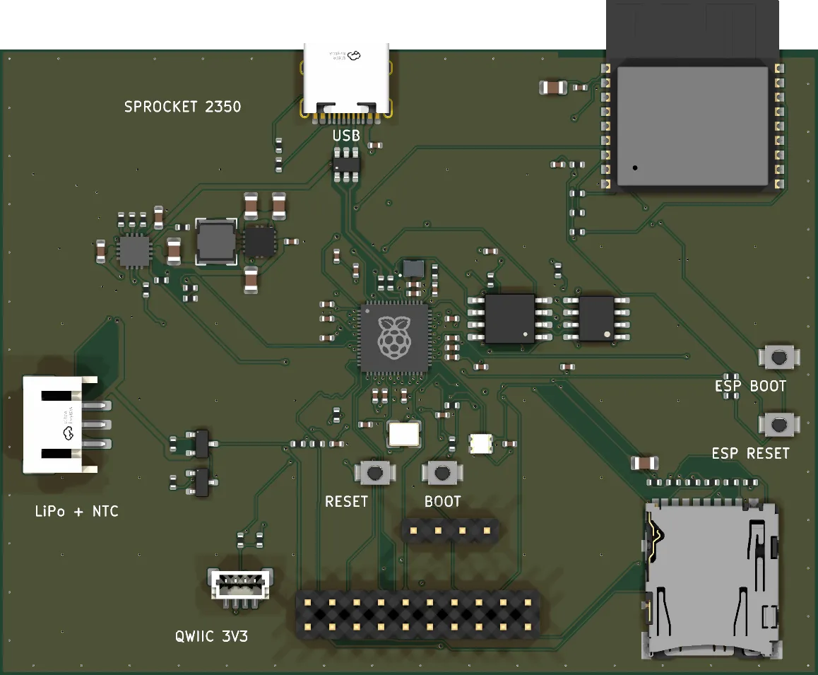
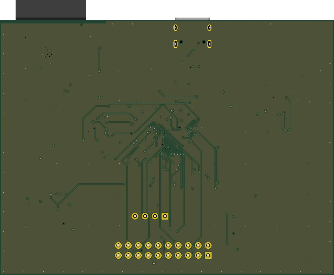
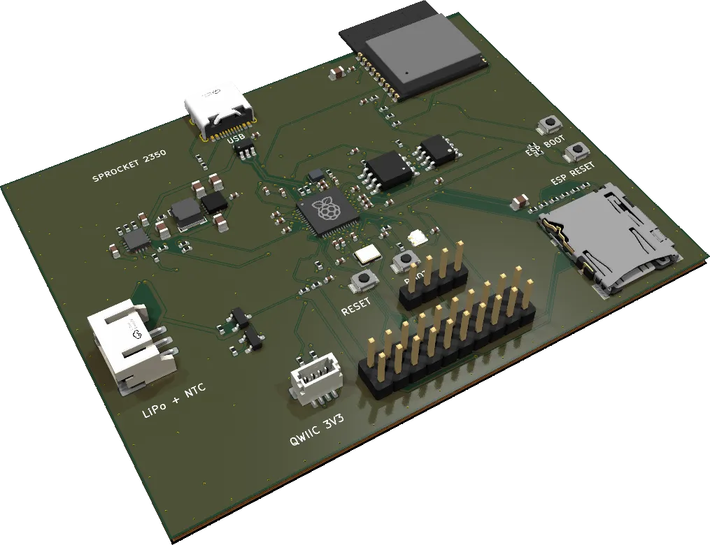
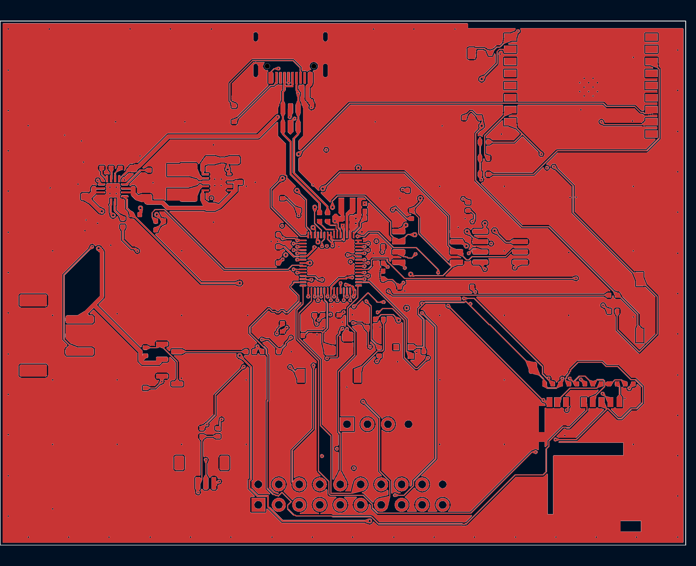
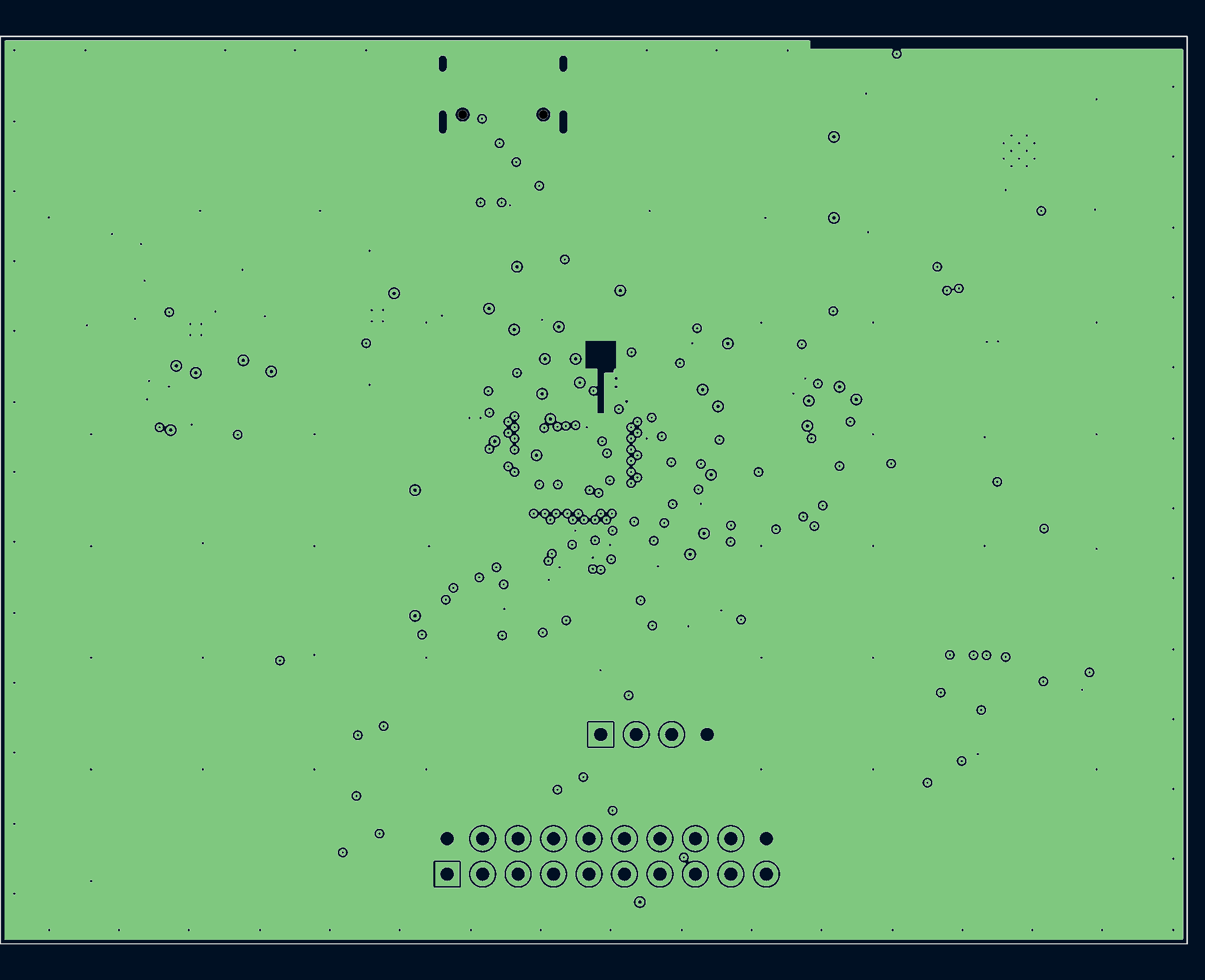
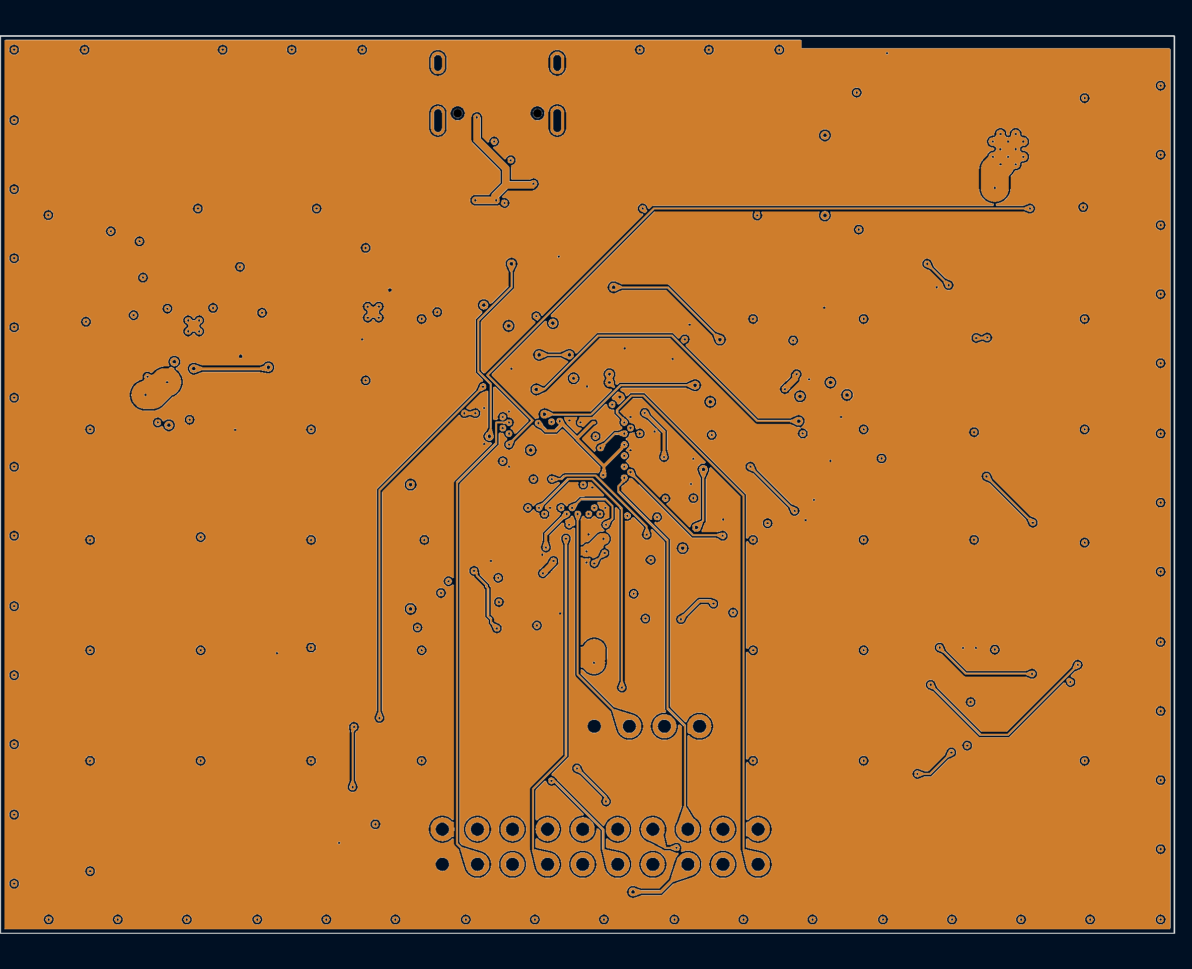
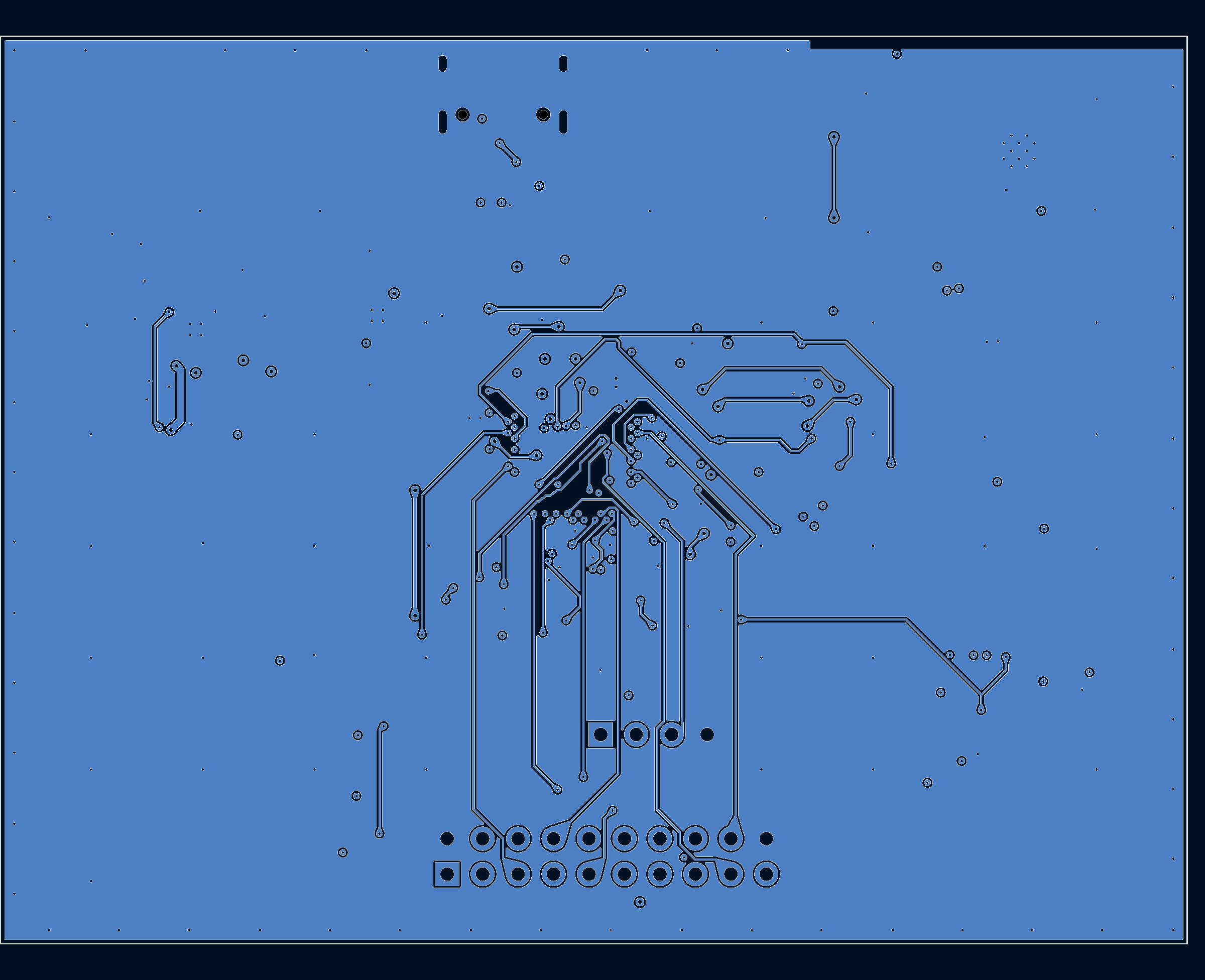
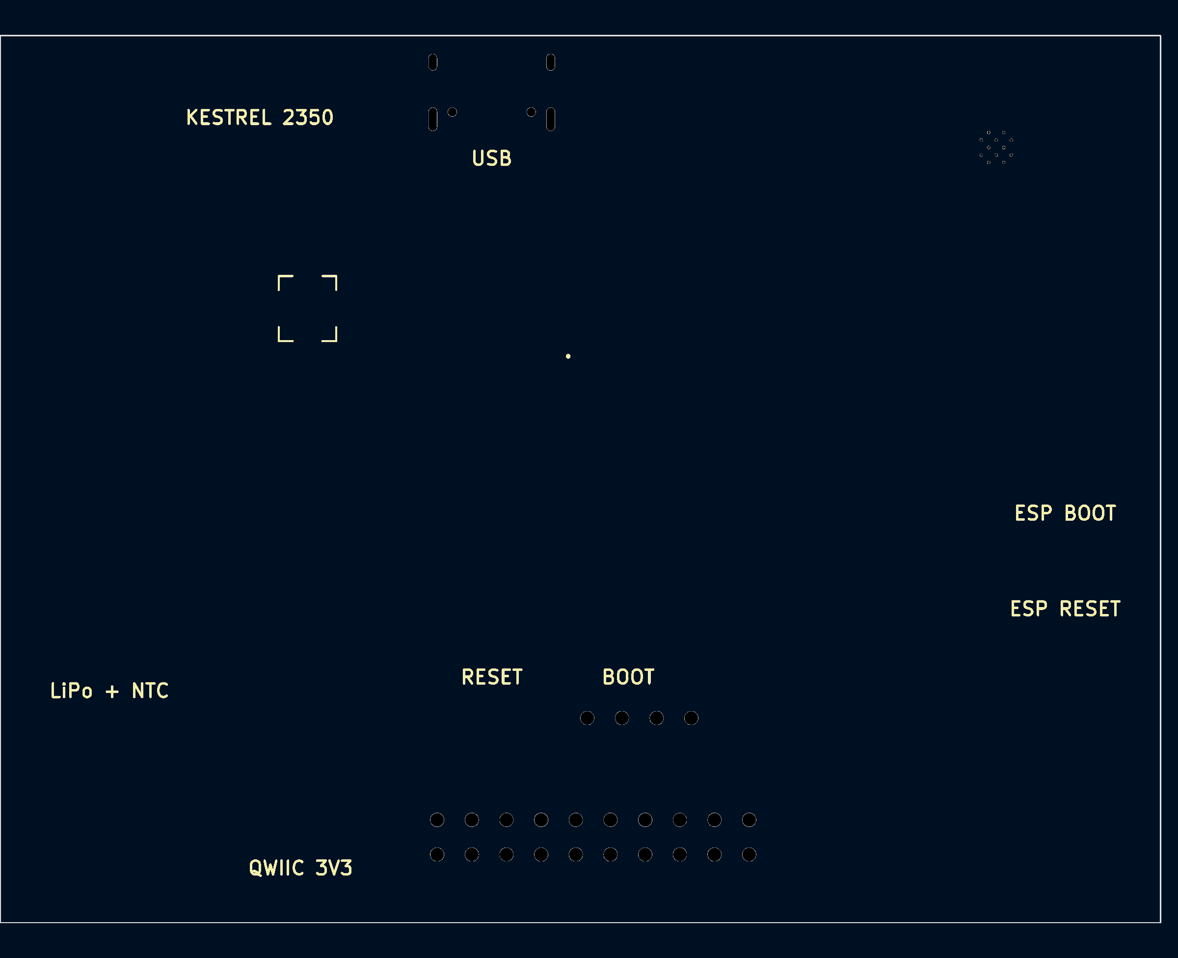
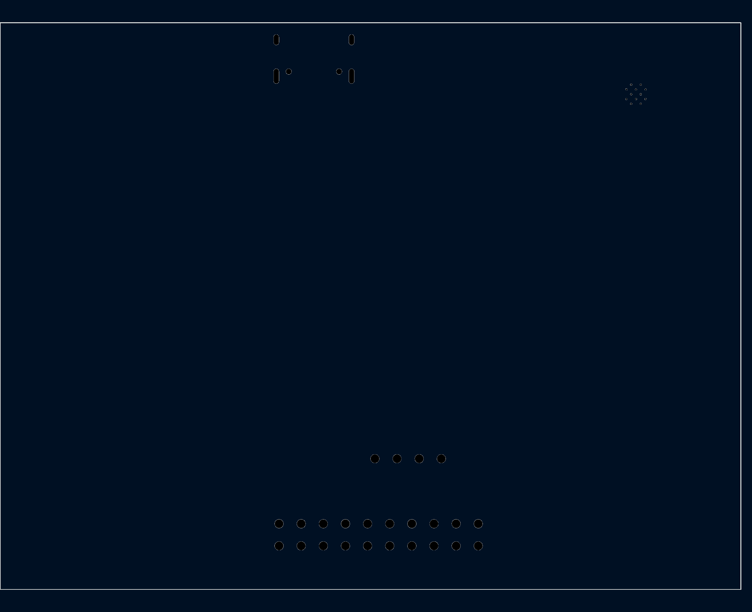
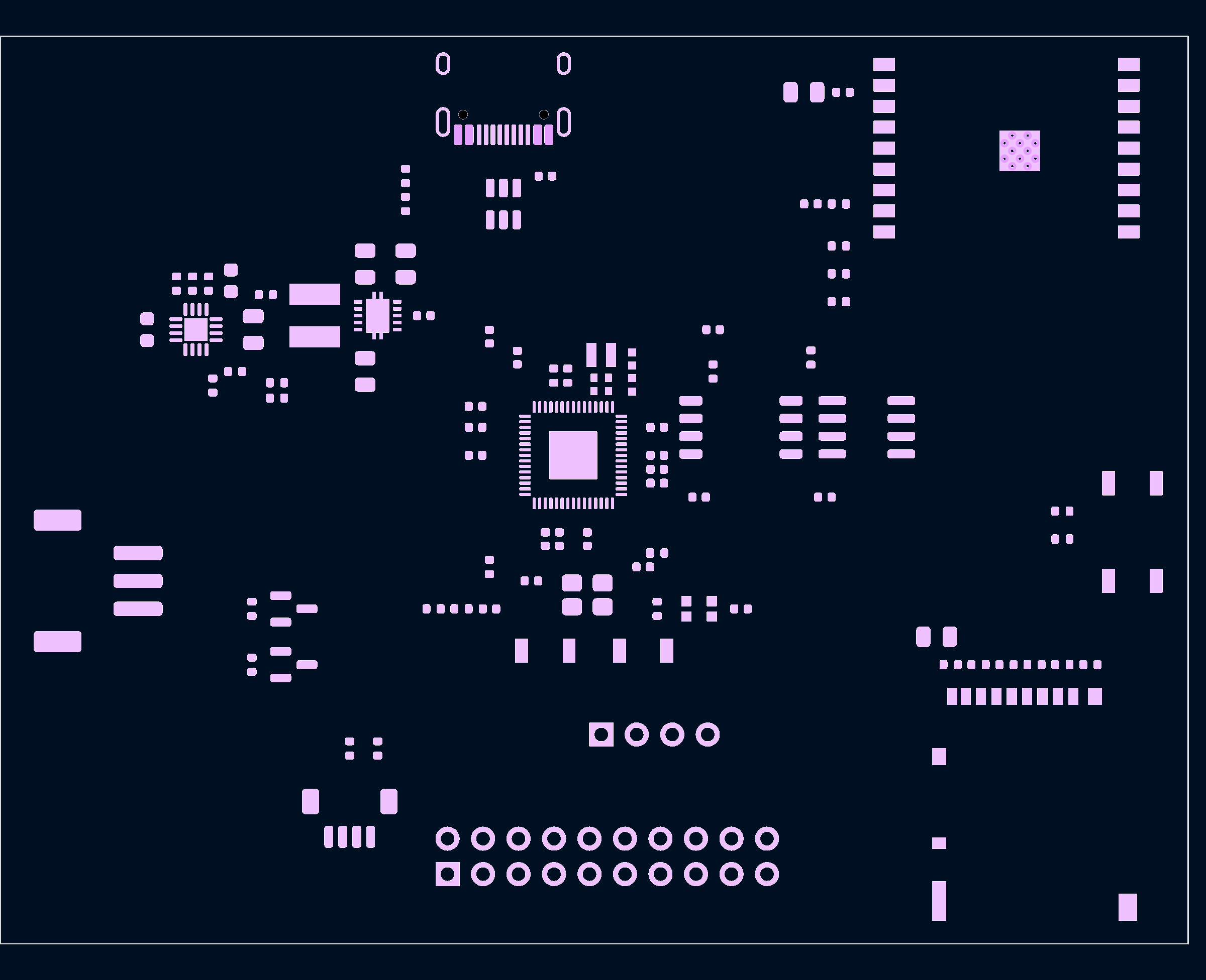
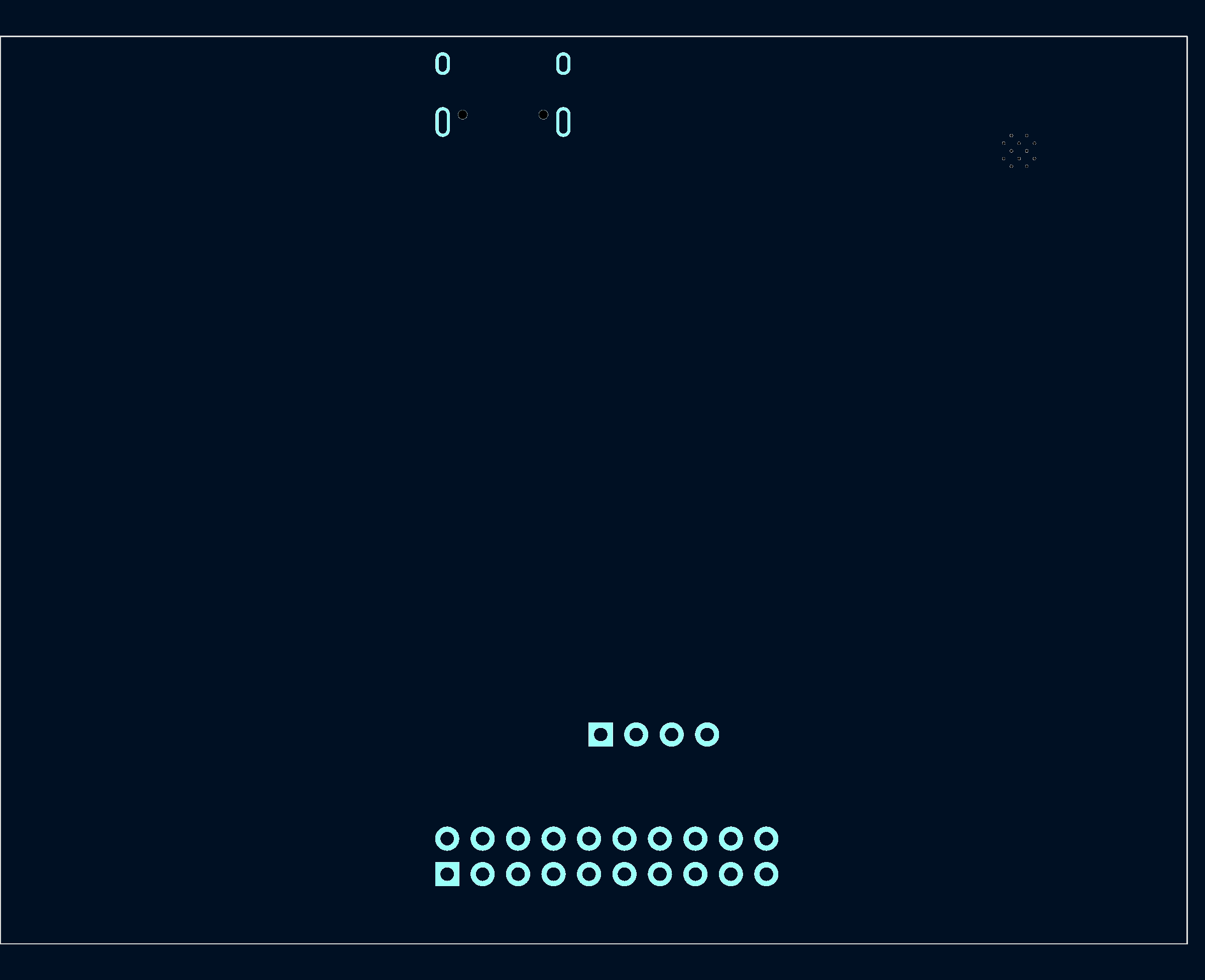
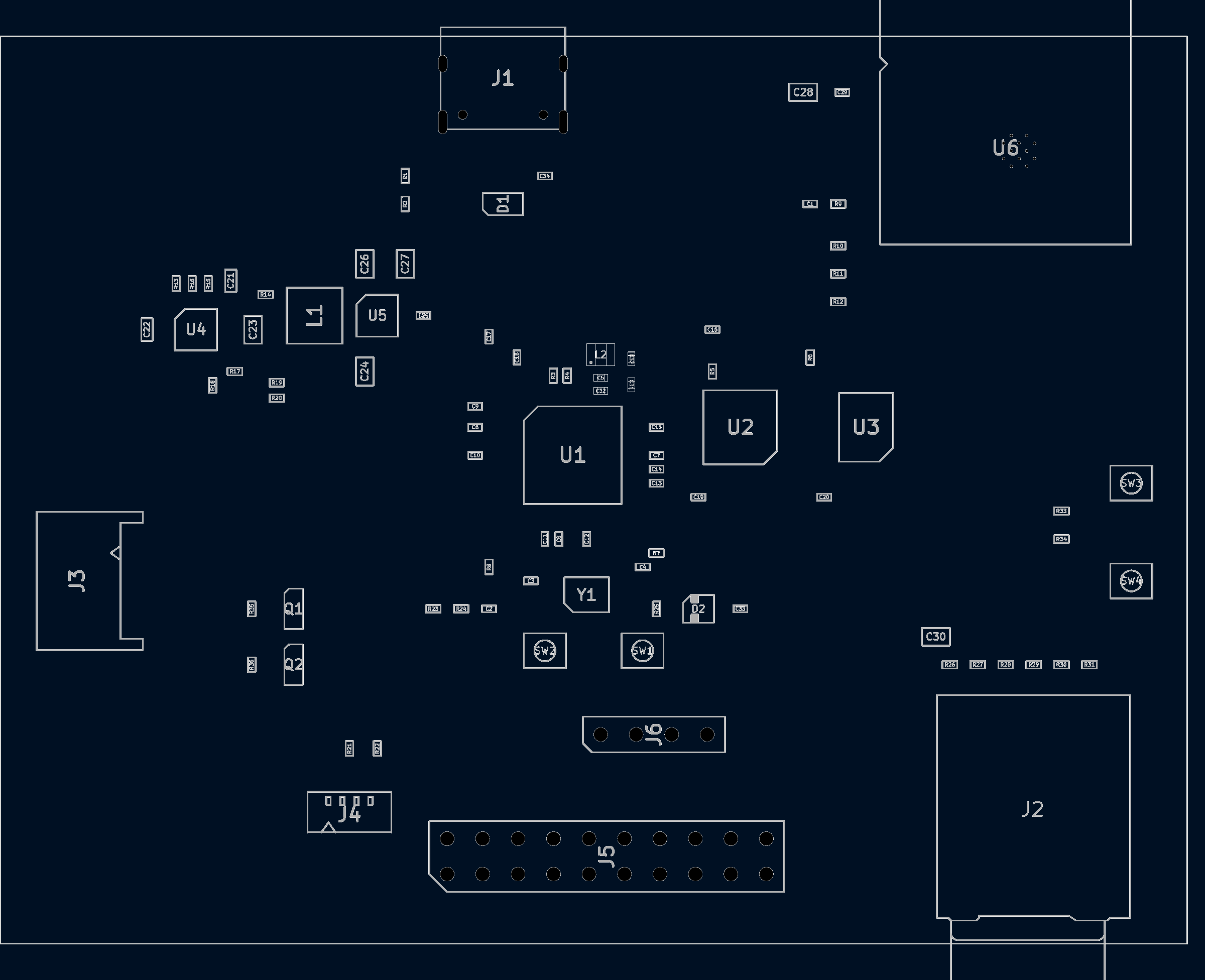
Rendered by kicad-cli with the run's own KiCad version. Dimensions in mm. The layers are the plots the AI judge saw, seen from the top, with their white background made dark. Click one to open it at full size.
- AI cost
- $53.72
- Time
- 1 h 36 min
- Tokens, incl. cache reads
- 185.1M
- 1 board
- $659.08
- 5 boards, per board
- $148.08
- Board size
- 85 × 65 mm
- Machine
- EC2 Ubuntu (c7i.2xlarge)
- sprocket
- sprocket 0.5.1
- kicadConnector
- v0.2.0
- kicad
- 10.99.0-6344-g8c85ac1452
Score
Design review8 of 20
- Layout7 of 101 minus 0.1 per minor and 0.2 per major layout finding, down to 0
- Routing1 of 10the same, for routing findings
Circuit checks19.3 of 20
- Decoupling4.3 of 5RP2350 power pins with a capacitor within 3.2 mm
- USB protection5 of 50.5 for an ESD part on D+ and D−, plus 0.25 for each line with a series resistor
- Antenna keepout5 of 51 when there are keepouts and no copper is in them
- Battery drain5 of 51 at 5 µA or less drawn by unswitched battery dividers, falling linearly to 0 at 25 µA
Layout checks19 of 30
- Thermal pads6 of 10mean over the exposed pads of their vias over the number needed, 0 for a pad with no plane on another layer
- Grounding7.7 of 10USB, QSPI and microSD track length over a ground plane on the next layer
- Silkscreen5 of 5texts at least 0.8 mm high
- Board size0.3 of 51 at the Feather RP2350's 50.8 × 22.8 mm area or less, falling linearly to 0 at 5 times that area
Orderable20 of 20
- Fab notes5 of 51 when every fab option in the notes can be ordered from PCBWay
- Board5 of 51 when the board needs no rework
- BOM lines10 of 101 minus 0.2 for each BOM line that needs a fix, down to 0
Parts data5 of 10
- 3D models5 of 5parts with a 3D model
- Supplier part numbers0 of 5BOM lines with a valid number from at least one supplier
| The five groups | 71.3 |
|---|---|
| Every gate passed, so no penalty | 0 |
| Score | 71.3 of 100 |
Gates
A board that fails a gate loses 20 points. The gates are the three checks below, every prompt feature, and any fatal review finding.
| Check | Result | What the check found |
|---|---|---|
| Crystal and load capacitors | Pass | Y1 ABM8-272-T3 (CL 10 pF) between XIN and XOUT via R25 1 kΩ; load caps /XIN: C3 15 pF; /XTAL_OUT: C4 15 pF; needs 10.5–17.5 pF per side for 3 pF stray |
| BOOTSEL and RUN buttons | Pass | QSPI_SS (/FLASH_CS) → R7 → SW1 → GND; RUN (/RUN) → SW2 → GND |
| Charger power path | Pass | U4 BQ24074RGTR: U4 IN (/VBUS) is on J1 VBUS; BAT (/BAT) goes to J3; U5 TPS63001DRCR makes /3V3 from OUT (/SYS) |
Prompt features
- Found RP2350 U1
- Found QSPI flash U2
- Found PSRAM U3
- Found USB-C J1
- Found Wi-Fi and BLE U6
- Found microSD J2
- Found Qwiic J4
- Found RGB LED D2
- Found Power-path charger U4
- Found Battery monitoring R23
Design review 8 of 20
Opus 5.5 reviewed an anonymous copy of the board and listed 9 findings. Layout and routing each start at 10 points.
Major
Routing
QSPI bus to flash and PSRAM takes long detours with several layer changes per line. The lines differ in length by up to about 3x, and each has 2 to 4 vias, which hurts signal integrity and timing margin at QSPI clock rates.
Evidence
U1 to U2 routed vs direct: D0 13.2 mm vs ~10 mm (2 vias); CLK 18.5 mm vs 9.6 mm (2 vias plus an In2.Cu hop (139,123.1)-(141.2,123.1)); D3 23.2 mm vs 9.4 mm (2 vias); D2 24.6 mm vs 17.6 mm (2 vias); D1 32.7 mm vs 18.1 mm (2 vias); FLASH_CS 41.2 mm vs 18.7 mm (3 vias). D1 runs from U1 pin 59 north to the via at (136.8,121), then on F.Cu along y=118.7 from x=142.1 to 150.1, then down to U2 pin 2. FLASH_CS goes west to (133.6,123.1)-(133.6,120.9), through the via at (135,119.5), along B.Cu to (143.1,119.5), along In2.Cu at y=118.2 to the via at (152.1,122), then to U2 pin 1. D2 runs ~23 mm on In2.Cu: (139.4,125.6)->(143.3,121.7)->(148.6,121.7)->(154.8,127.9). D3 detours north on B.Cu to (143.3,121.7) and leaves a 2.6 mm stub from the via at (151.5,128.9) to U2 pin 7. U1 to U3 (PSRAM) totals are 24-43 mm with 3-4 vias per line. PSRAM_CS (U1 pin 2) is 43.6 mm, including an 18.7 mm B.Cu run at y=121.3.
The microSD SPI bus wanders around the board. SD_CLK is more than twice the direct distance, and the bus lines differ greatly in length and via count.
Evidence
SD_CLK from U1 pin 14 (137.55,132.4) to J2 pin 5 (172.4,147.3) is 83.2 mm against ~38 mm direct, all on F.Cu. It runs down x~133.1 to y~158, along y=161.35-162.35 under J5 to (157.8,162.35), then back up to J2. SD_MOSI from U1 pin 15 to J2 pin 3 is 69.8 mm with 2 vias and runs along y=161.05 from x=146.8 to 158.35. SD_MISO is 44.8 mm with 4 vias. SD_CS from U1 pin 13 to J2 pin 2 is 49.7 mm with 6 vias.
The crystal drive path from XOUT through R25 to Y1 is long and changes layers six times, including an inner-layer segment. This adds parasitic capacitance and noise pickup to the oscillator loop and makes it asymmetric with XIN.
Evidence
XOUT: U1 pin 22 (140.6,133.45) -> via (140.6,134.175) -> B.Cu (141.65,133.15)-(143.8,133.15) -> via (145.4,134.75) -> F.Cu to R25 at (147,140.5). That is 13.0 mm with 2 vias. XTAL_OUT from Y1 pin 3 to R25 is 8.1 mm with 4 vias at (143,138.2), (143.75,137.45), (145.85,140.4) and (146.7,142.2), partly on In2.Cu (143.75,137.45)-(143,138.2). The total path is ~21 mm with 6 vias. XIN is 8.1 mm with 0 vias.
Minor
Layout
Flash U2 and PSRAM U3 are placed far east of the RP2350 QSPI pins, with capacitors between them. This placement forces the long QSPI routes.
Evidence
The QSPI pins are on U1's north side at y=126.55, x=138.2-140.2. U2 at (153,128) has pads 10-18 mm from those pins, center 13.7 mm. U3 at (162,128) has pads 20.6-25.6 mm away, center 22.6 mm. C13-C15 sit between U1 and the memories.
Crystal Y1 is placed behind the decoupling capacitors instead of next to XIN/XOUT, and R25 is offset to the east. This placement forces the long crystal route.
Evidence
Y1 at (142,140) is ~5.7-7.4 mm from U1 pins 21/22 at y=133.45. C11, C8 and C12 sit between Y1 and U1. R25 is at (147,141).
Charger U4 is placed ~26 mm from the USB-C VBUS pins, although the area next to J1 is empty. The long VBUS run goes through vias.
Evidence
U4 at (114,121); J1 VBUS pads at x 133.55-138.45, y 107.05. The routed VBUS path from J1 A4 to U4 pin 13 is 26.9 mm through 2 vias. The area x 115-130, y 100-112 next to J1 is empty. U5 is at (127,120).
Routing
SD_MOSI continues past the card connector pin as a ~21 mm stub to reach its pull-up resistor R27, which sits far from J2.
Evidence
After J2 pin 3 (174.6,147.45) the trace continues (176.6,149.3)->(179.65,147.35)->(179.65,145.35)->(178.2,144.45)->(176.6,142.85)->(174.6,142.3)->(171.65,142.3) and ends at R27 pad 2 (170.51,145). The routed length from J2 pin 3 to R27 is 21.3 mm.
The VBUS feed to the charger necks down to 0.11 mm traces and single small vias. This is marginal for the 500 mA input limit and the USB inrush current.
Evidence
The last 0.7 mm into U4 pin 13 (114.75,119.56) is 0.11 mm wide: (115.25,119.1)->(114.8,119.55). The pad itself is 0.25 mm wide. J1 A9/B4 joins through a 0.11 mm trace (133.6,107)->(133.6,106.3)->(134,105.9)->(134.425,105.9) to the via at (134.5,105.9). The path passes through single 0.45/0.2 mm vias at (138.6,110.7) and (134.4,111.9). Input current is up to 500 mA because EN2 is tied to GND and EN1 is driven by GP6 (bq24074 Table 7-2).
The buck-boost U5 output reaches the 3V3 plane through one thin trace and one via that also carries the FB connection. Load current shares the feedback path, and there is no via at the output capacitors.
Evidence
U5 VOUT connects to the In2.Cu 3V3 plane only through a 0.2 mm x 1.2 mm trace (128.2,117.25)->(128.2,118.4) and one 0.6/0.3 mm via at (128.2,118.4). This is also the path to FB pin 10. C26 and C27 have no via to the plane.
Opus 5.5's notes
The review found 9 confirmed problems: 4 major and 5 minor, with no fatal faults. They're in review.json, which is valid JSON. I've also deleted the scratch folder and the pickle cache.
The upgrade made no changes. kicad-cli reported that the schematic and board are already in the connector's latest format (KiCad 10.99), so I didn't touch either file. DRC reports no violations and no unconnected items. The footprints and the pinouts of the main ICs match their libraries and datasheets.
| # | Area | Severity | Refs | Problem |
|---|---|---|---|---|
| 1 | routing | major | U1, U2, U3 | QSPI lines are 13–41 mm long to the flash against 9–19 mm direct, with 2–4 vias each. Lines to the PSRAM are 24–44 mm. |
| 2 | routing | major | U1, J2 | SD_CLK is 83 mm against about 38 mm direct, and the rest of the SD bus is 45–70 mm with up to 6 vias. |
| 3 | routing | minor | J2, R27 | SD_MOSI runs on past the card pin as a 21 mm stub to its pull-up. |
| 4 | routing | major | U1, R25, Y1, C4 | The crystal output path is about 21 mm with 6 vias, one segment on an inner layer. XIN is 8 mm with no vias. |
| 5 | layout | minor | U1, U2, U3 | Flash and PSRAM sit 14–23 mm from the QSPI pins. |
| 6 | layout | minor | Y1, R25 | The crystal sits 6–7 mm away, behind the decoupling caps. |
| 7 | layout | minor | U4, J1 | The charger is 26 mm from the USB-C VBUS pins, and the area next to J1 is empty. |
| 8 | routing | minor | J1, U4 | The VBUS feed narrows to 0.11 mm traces and passes through single 0.2 mm vias. |
| 9 | routing | minor | U5, C26, C27 | The 3V3 output reaches its plane through one 0.2 mm trace and one via, which it shares with the feedback pin. |
I chose not to report these:
- Battery and system power traces: their width is adequate for the current they carry.
- J4 and SW1/SW2: they sit inside the board but can still be reached.
- Q2: its gate is tied to 3V3, so battery sensing is always on. That isn't a fatal fault, and the "other" area only takes fatal ones.
Circuit checks 19.3 of 20
Decoupling
4.3 of 512 of 14 RP2350 power pins have a capacitor within 3.2 mm.
| Pin | Pad | Net | Nearest capacitor | Distance |
|---|---|---|---|---|
| IOVDD | 1 | /3V3 | C9 | 3.15 mm |
| DVDD | 6 | /1V1 | C6 | 3.3 mm |
| IOVDD | 11 | /3V3 | C10 | 3.3 mm |
| IOVDD | 20 | /3V3 | C11 | 2.22 mm |
| DVDD | 23 | /1V1 | C8 | 2.3 mm |
| IOVDD | 30 | /3V3 | C12 | 2.74 mm |
| IOVDD | 38 | /3V3 | C14 | 2.3 mm |
| DVDD | 39 | /1V1 | C7 | 2.11 mm |
| ADC_AVDD | 44 | /3V3 | C15 | 2.11 mm |
| IOVDD | 45 | /3V3 | C32 | 2.04 mm |
| VREG_AVDD | 46 | /VREG_AVDD | C31 | 1.8 mm |
| VREG_VIN | 49 | /3V3 | C32 | 1.17 mm |
| USB_OTP_VDD | 53 | /3V3 | C32 | 1.88 mm |
| QSPI_IOVDD | 54 | /3V3 | C32 | 2.21 mm |
USB protection
5 of 5- ESD parts on D+ and D−
- D1
- D+ nets, connector to RP2350
- /USB_CONN_DP → /USB_DP series resistor
- D− nets, connector to RP2350
- /USB_CONN_DM → /USB_DM series resistor
Differential pair, not scored
- D+ and D− length
- 23.84 mm and 25.79 mm
- Mismatch
- 1.95 mm
- Vias
- 2
- Longest coupled stretch
- 8.76 mm on F.Cu, 0.22 mm wide, 0.15 mm gap
- Differential impedance
- 90.7 Ω
Antenna keepout
5 of 51 keepout covers the Wi-Fi module U6.
| Keepout | Layers | Copper inside |
|---|---|---|
| U6 footprint | F.Cu, B.Cu, In1.Cu, In2.Cu | none |
Battery drain
5 of 5Unswitched dividers draw 0 µA from a full battery, even when the board is off.
| Divider | Buffered by | Switched by | At 4.2 V |
|---|---|---|---|
| R23 100k / R24 100k | none | Q1 | 21 µA |
Layout checks 19 of 30
Thermal pads
6 of 10| Exposed pad | Net | Vias | Needed | Plane on another layer |
|---|---|---|---|---|
| U1 | /GND | 0 | 9 | yes |
| U4 | /GND | 4 | 5 | yes |
| U5 | /GND | 4 | 4 | yes |
Grounding
7.7 of 10| Bus | Over ground | Track length | Share |
|---|---|---|---|
| USB | 46.3 mm | 49.6 mm | 93.3% |
| QSPI | 137.7 mm | 215.6 mm | 63.9% |
| microSD | 277.8 mm | 336.3 mm | 82.6% |
| All three | 461.8 mm | 601.5 mm | 76.8% |
Silkscreen
5 of 50 of 8 texts are below PCBWay's 0.8 mm minimum. The smallest is 1 mm.
Board size
0.3 of 585 × 65 mm, 5525 mm². The Feather RP2350 is 50.8 × 22.8 mm.
Orderable 20 of 20
| 1 board | 5 boards | |
|---|---|---|
| PCBs | $526.83 | $526.83 |
| Assembly | $88.00 | $96.10 |
| Components | $44.25 | $117.46 |
| Total | $659.08 | $740.39 |
| Per board | $659.08 | $148.08 |
PCBWay's instant quote for the options in the fab notes, without shipping. PCBWay makes at least 5 PCBs, so 1 board is 5 PCBs with 1 assembled. Parts are at distributor list prices.
Fab notes
5 of 5No fixes needed.
Board
5 of 5No fixes needed.
BOM lines
10 of 100 of 55 BOM lines need a fix.
Parts data 5 of 10
3D models
5 of 5Every part has a 3D model.
Supplier part numbers
0 of 50 of 55 BOM lines have a valid supplier part number.
LCSC 0%, Digi-Key 0%, Mouser 0%
Stock
100% of 55 BOM lines are stocked for 5 boards at LCSC, JLCPCB or Digi-Key.
| Parts | MPN | At |
|---|---|---|
| C1 C20 | GRM155R61A105KE15D | Digi-Key |
| C18 | GRM155R61A105KE15D | Digi-Key |
| C21 C22 | GRM188R61A475KE15D | Digi-Key |
| C23 | GRM21BR61A106KE19L | Digi-Key |
| C24 | GRM21BR61A106KE19L | Digi-Key |
| C28 | GRM21BR61A106KE19L | Digi-Key |
| C30 | GRM21BR61A106KE19L | Digi-Key |
DRC and ERC
| Errors | Warnings | Unconnected | |
|---|---|---|---|
| DRC | 0 | 0 | 0 |
| ERC | 0 | 0 |
Files
The agent's README
Sprocket 2350
RP2350A development board with 16 MiB QSPI flash, 8 MiB PSRAM, USB-C device interface, rechargeable single-cell battery power, ESP32-C3 Wi-Fi/BLE, SPI microSD, Qwiic/STEMMA QT and an addressable RGB indicator.
Release status
Prototype design. No hardware has been built or tested. The revised layout uses the Raspberry Pi regulator core, a compact charger/buck-boost stage, local radio bypassing and a shorter USB route. The files in fab/ support PCBWay's prototype quote and engineering review. They do not establish bench performance or manufacturer acceptance.
Before ordering, PCBWay must confirm exact sourcing, controlled impedance, filled/capped vias and complete assembly. Qualify the built prototype before production release. See release-review.md.
Design choices
| Item | Choice |
|---|---|
| MCU | Bare RP2350A, current stepping to be confirmed by supplier |
| Memory | W25Q128JVSIQ flash; APS6404L-3SQR-SN PSRAM on shared QSPI bus with GPIO0 CS1 |
| Radio | ESP32-C3-WROOM-02-N4, integrated antenna beyond the PCB edge |
| Power | BQ24074 power-path charger, approximately 303 mA charge setting; TPS63001 fixed 3.3 V buck-boost |
| Battery | External protected 1S 4.2 V LiPo pack, cell-mounted 10 kΩ B3435 NTC, keyed 3-pin JST PH |
| PCB | 85 × 65 mm, four copper layers, top-side components and two factory-installed through-hole headers |
| Debug | RP2350 SWD header; RP BOOTSEL/reset and ESP boot/reset buttons |
| RGB | WS2812C-2020-V6, manufacturer-supported 3.3 V operation, not an older WS2812 substitution |
PCBWay must source and install every BOM reference, including headers J5/J6. No part is reserved for user assembly.
Interfaces and firmware
| Function | RP2350 GPIO |
|---|---|
| PSRAM CS | 0, QMI CS1n |
| Qwiic SDA / SCL | 2 / 3, I²C1 |
| ESP RX / TX | RP TX 4 → ESP RX20; RP RX 5 ← ESP TX21, UART1 |
| microSD MISO / CS / CLK / MOSI | 8 / 9 / 10 / 11, SPI1 |
| RGB data | 20, PIO |
| ESP EN / BOOT | 23 / 24. Drive EN high to enable; drive BOOT low/release for download mode. |
| USB input limit | 6. Low/high impedance selects USB100; high selects USB500. J5 pin 4 is unused. |
| Card detect | 25, low when inserted |
| Battery monitor | 26 / ADC0, VBAT = 2 × measured ADC voltage |
Initialize PSRAM through QMI. Observe the manufacturer's startup/reset, refresh and maximum chip-select duration limits. Begin with conservative QSPI and SD clock rates. The ESP module needs application firmware or a compatible ESP-AT build. RP firmware can bridge the UART to program the ESP while controlling its boot/reset pins. No firmware image is included or tested.
Hold RP BOOTSEL while releasing RESET to enter the USB ROM loader. BOOTSEL alone does not reset the MCU. SWD reference voltage is an output, not a board power input.
Expansion header J5
Numbering follows the square pin-1 pad on the assembly drawing. All signals are 3.3 V.
| Odd pin | Signal | Even pin | Signal |
|---|---|---|---|
| 1 | 3V3 output | 2 | GND |
| 3 | GP1 | 4 | Unused |
| 5 | GP7 | 6 | GP15 |
| 7 | GP16 | 8 | GP17 |
| 9 | GP18 | 10 | GP19 |
| 11 | GP12 | 12 | GP13 |
| 13 | GP14 | 14 | GP22 |
| 15 | CHG, active low | 16 | GP21 |
| 17 | GP27 / ADC1 | 18 | GP28 / ADC2 |
| 19 | GP29 / ADC3 | 20 | GND |
J6 pins 1–4 are 3V3 reference output, SWDIO, SWCLK and GND. J4 pins 1–4 are GND, 3V3 output, SDA and SCL.
Power and safety limits
- USB is a 5 V sink/device, not USB PD and not a host. Separate 5.1 kΩ CC resistors are fitted.
- Startup selects USB100 and holds the ESP disabled. Firmware may drive GP6 high only after the source permits 500 mA. Keep GP23 low until the supply budget allows radio operation. Do not enable the radio, SD writes or external Qwiic loads on a 100 mA budget.
- This prototype does not guarantee generic legacy-host pre-enumeration or suspend compliance. SD, RGB and Qwiic power are not hardware-gated, and the ROM loader does not implement this board's power policy. Use a source explicitly allowing 500 mA for USB-only development, or a protected battery with a qualified USB host. Do not advertise USB certification.
- The 500 mA USB budget includes both system load and charging. The charger reduces charging and can supplement from the battery. Wi-Fi transmission, SD writes and Qwiic loads must be qualified together. Do not assume USB-only operation supports every combined peak.
- Use a protected 4.2 V single-cell pack that permits at least 335 mA charging and the measured peak discharge current. The board charger is not pack overdischarge or short-circuit protection.
- J3 pin 1 is BAT+, pin 2 GND, pin 3 NTC. NTC must connect to GND in the pack and contact the cell. This is not a standard two-wire JST battery pinout. Check polarity before connecting.
- The direct NTC circuit allows approximately 0–50°C charging, with tolerance. Only use cells qualified for that range; cells limited to 45°C need tighter charge inhibition.
- Battery monitoring uses a PMOS switch enabled from the live 3.3 V rail through an NMOS. This avoids an always-connected battery divider when the MCU is unpowered. Its startup/shutdown transient still needs bench validation.
- Do not drive GPIO, SWD, I²C or UART from powered external equipment while the board is unpowered. Expansion pins are 3.3 V interfaces. Do not inject power through J4/J5/J6.
- WS2812C-V6's below-3.3 V behavior is not specified. Qualify indicator operation at worst-case rail tolerance and temperature. Do not substitute older 5 V-only LED revisions.
Manufacturing files
Open sprocket2350.kicad_pro with KiCad 10.99 or a compatible newer release. Embedded symbols and footprints allow inspection without regeneration. Generation tools use the connector's kicad-python, headless API and KiCad 10 library tables.
Fabrication package, BOM, assembly instructions and procurement checks are in fab/. The package includes Gerbers, drills, position CSV, schematic PDF, assembly drawings and check reports for review.
Final all-severity ERC and DRC report zero violations, zero opens and zero schematic parity issues under the project's recorded check settings. The BOM, schematic, PCB and placement file agree on all 93 fitted references. All component model files exist. The package identifies 18 vias requiring filled/capped processing.
PCBWay must confirm sourcing in its quote; distributor stock is not PCBWay inventory. No quote or order has been placed.
Review before release
- Review final ERC/DRC reports, confirm complete routing and accept zero opens/shorts. Review all warnings; do not dismiss physical violations as library noise.
- Verify L2's lower-left winding dot on the assembly drawing. Check filled/capped vias and the charger/regulator paste process.
- Have PCBWay confirm the proposed four-layer stackup and 90 Ω ±10% USB impedance. The nominal dielectric dimensions are a quote target, not a field-solver or manufacturer sign-off.
- Verify footprints and pin 1 against ordered USB, JST, SD and QFN package drawings. RF antenna area must remain copper- and enclosure-free.
- Confirm component sourcing, full through-hole assembly and panel rails/fiducials with PCBWay.
- After building an accepted prototype, test USB enumeration in both plug orientations, ROM boot/SWD, flash/PSRAM stress, SD writes, Wi-Fi/BLE, RGB, Qwiic, battery ADC and all USB/battery insertion sequences. Test NTC open/short and charger current/temperature before production release.