Rank 1 of 7 in RP2350 dev board
Opus 5.5 in Sprocket
Anthropic's Opus 5.5 on medium reasoning, in Sprocket CLI with its KiCad connector.
81.2 of 100
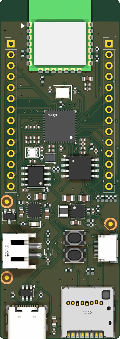
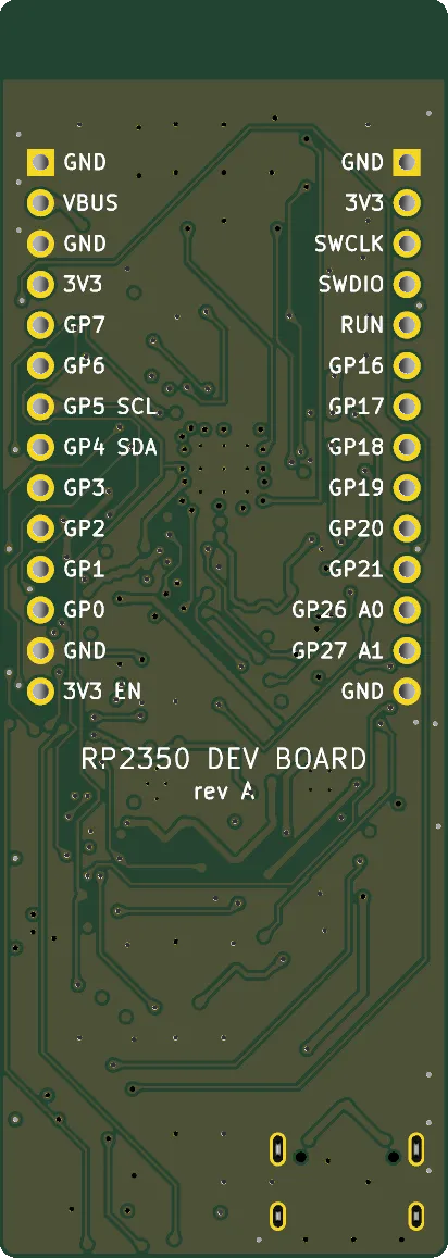
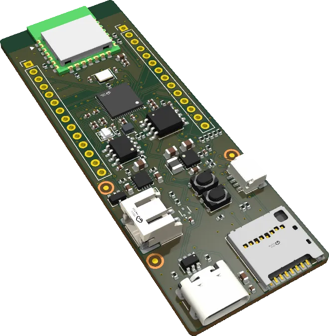
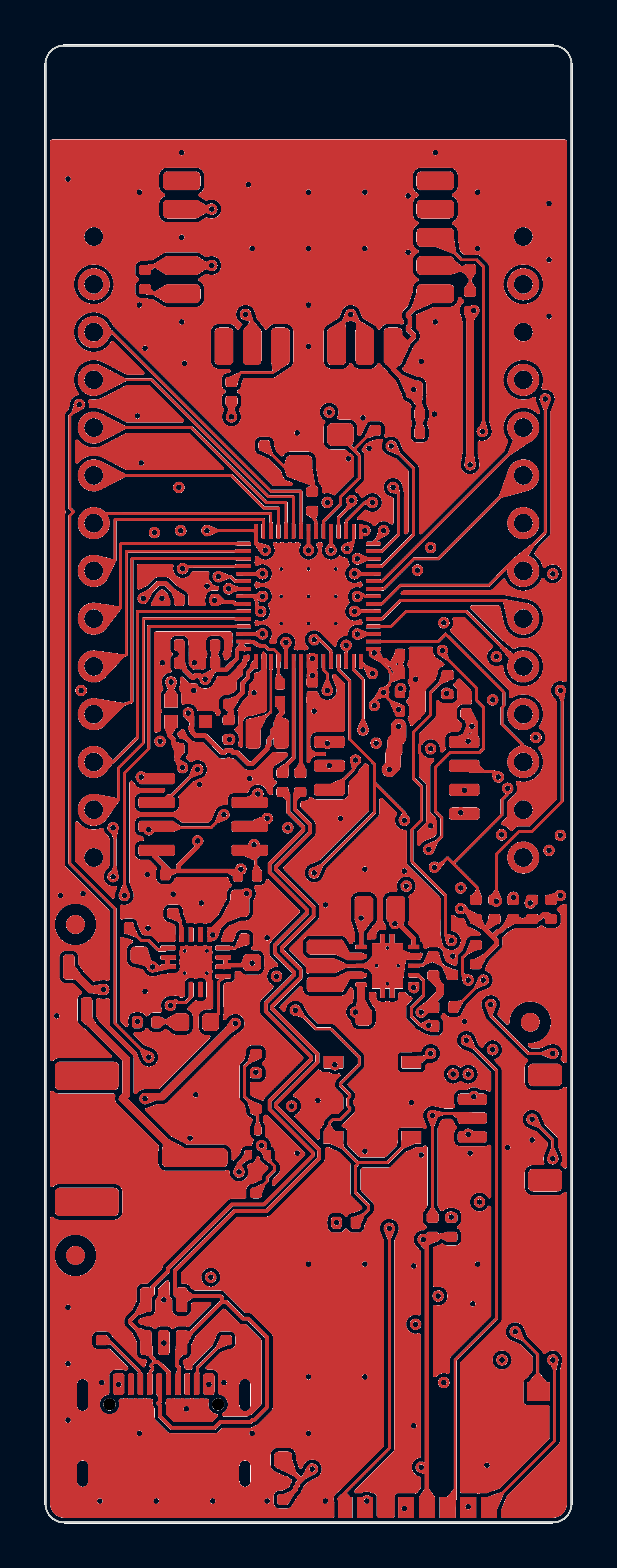
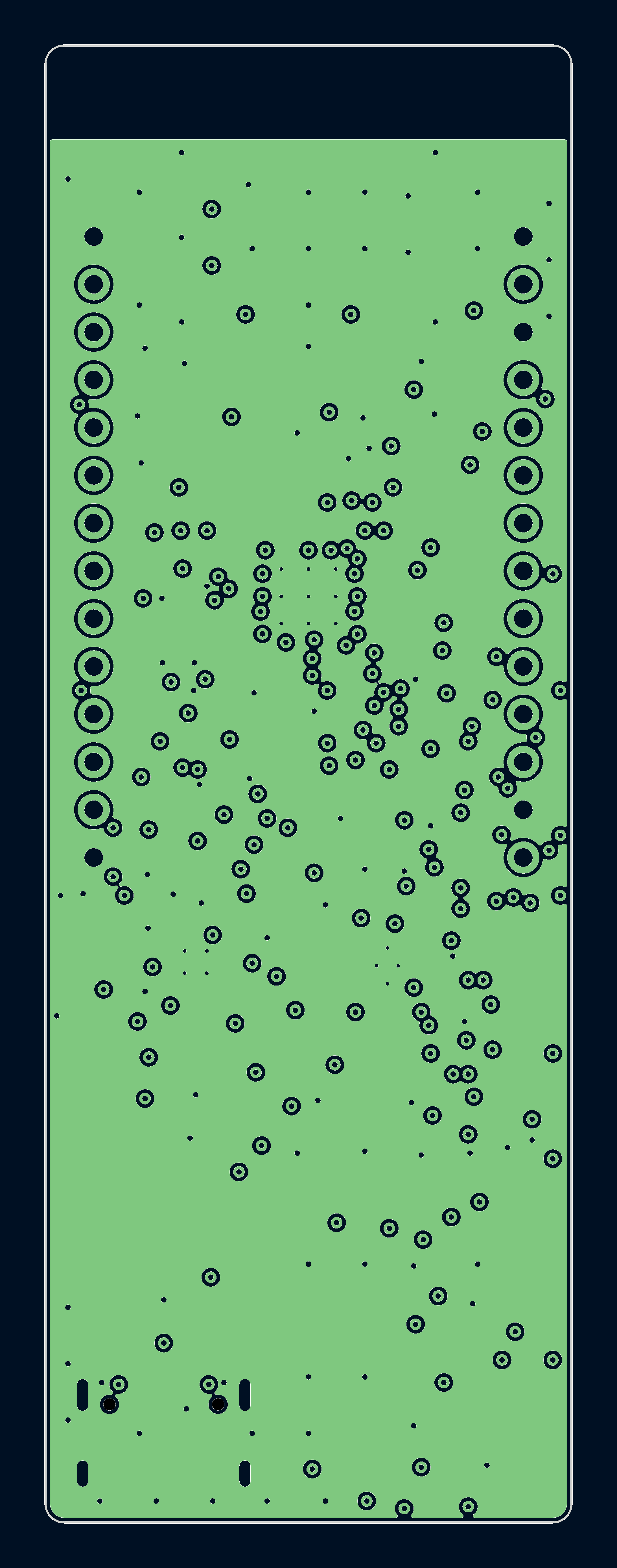
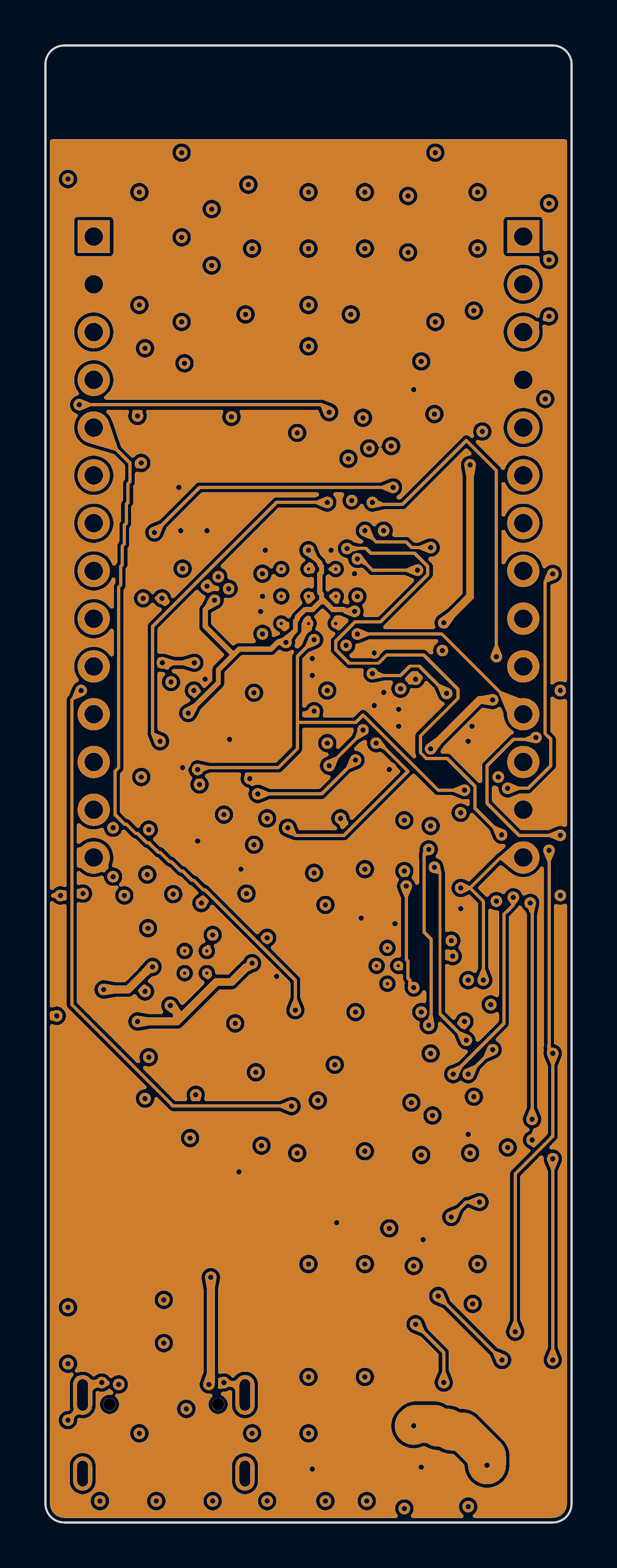
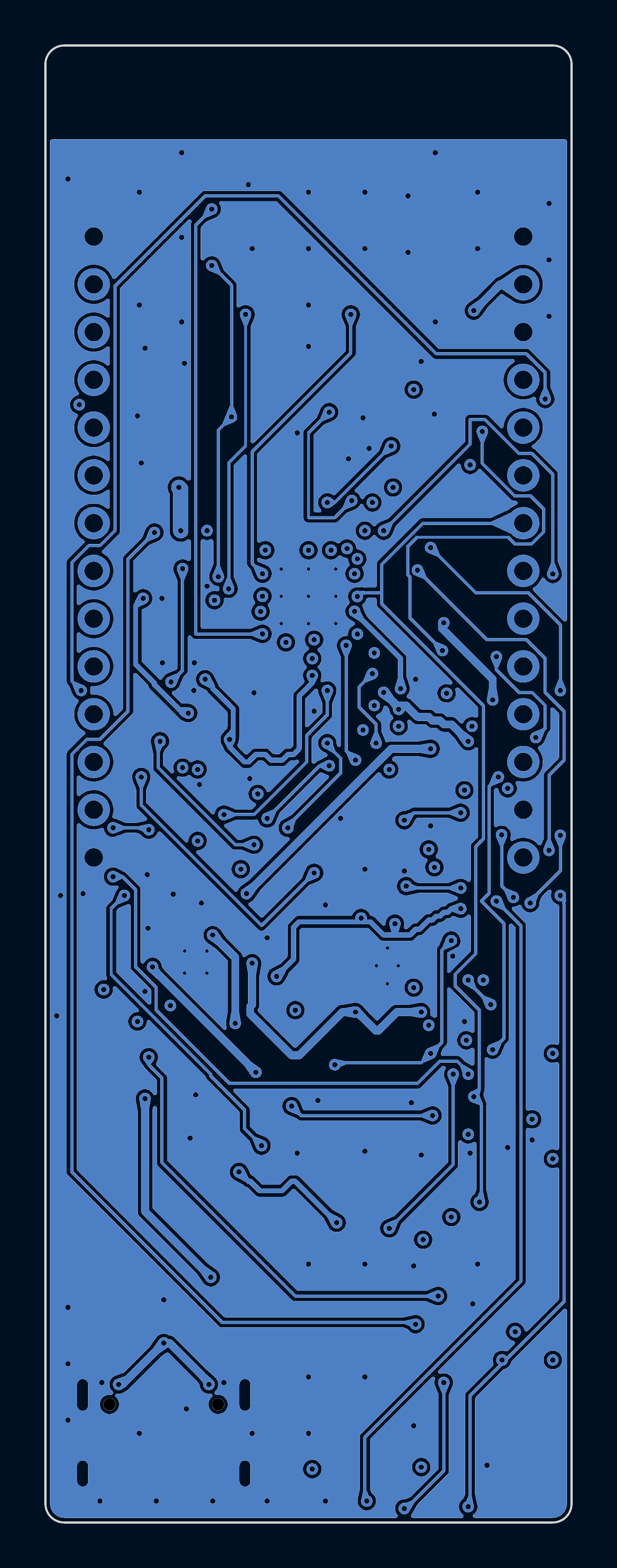
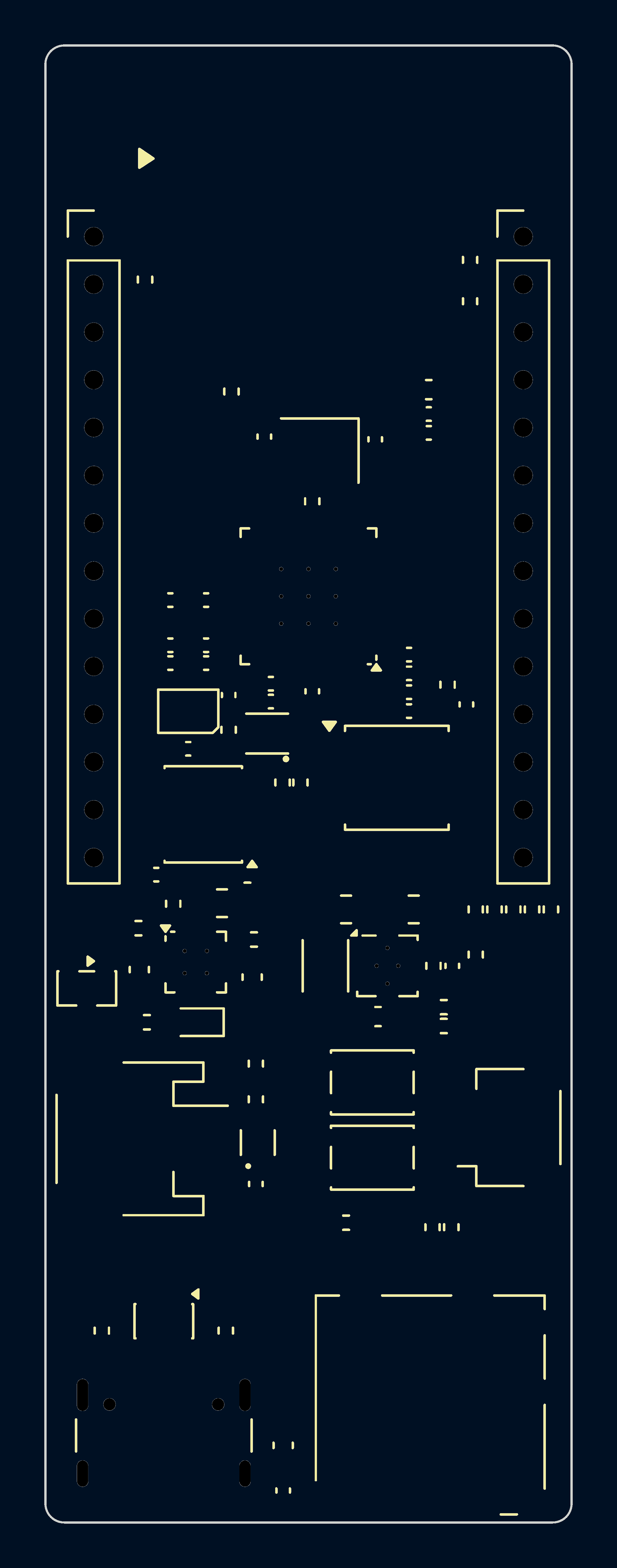
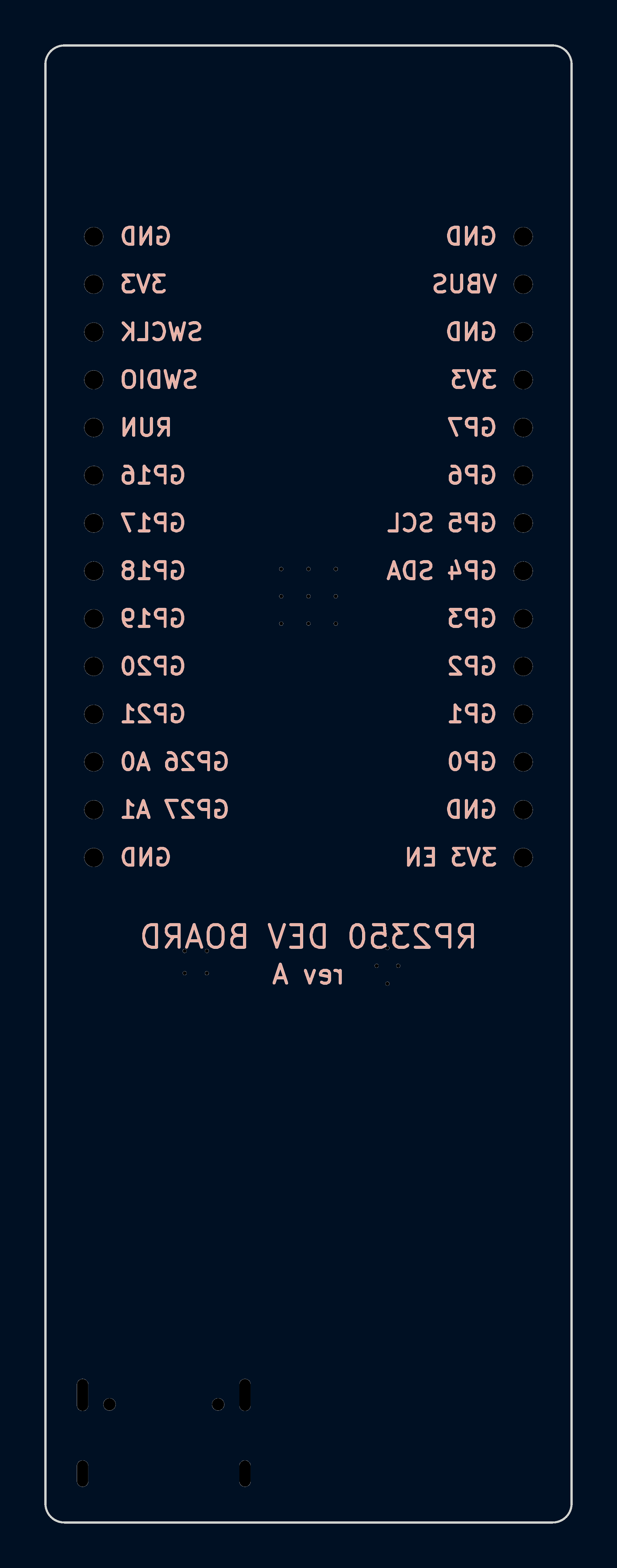
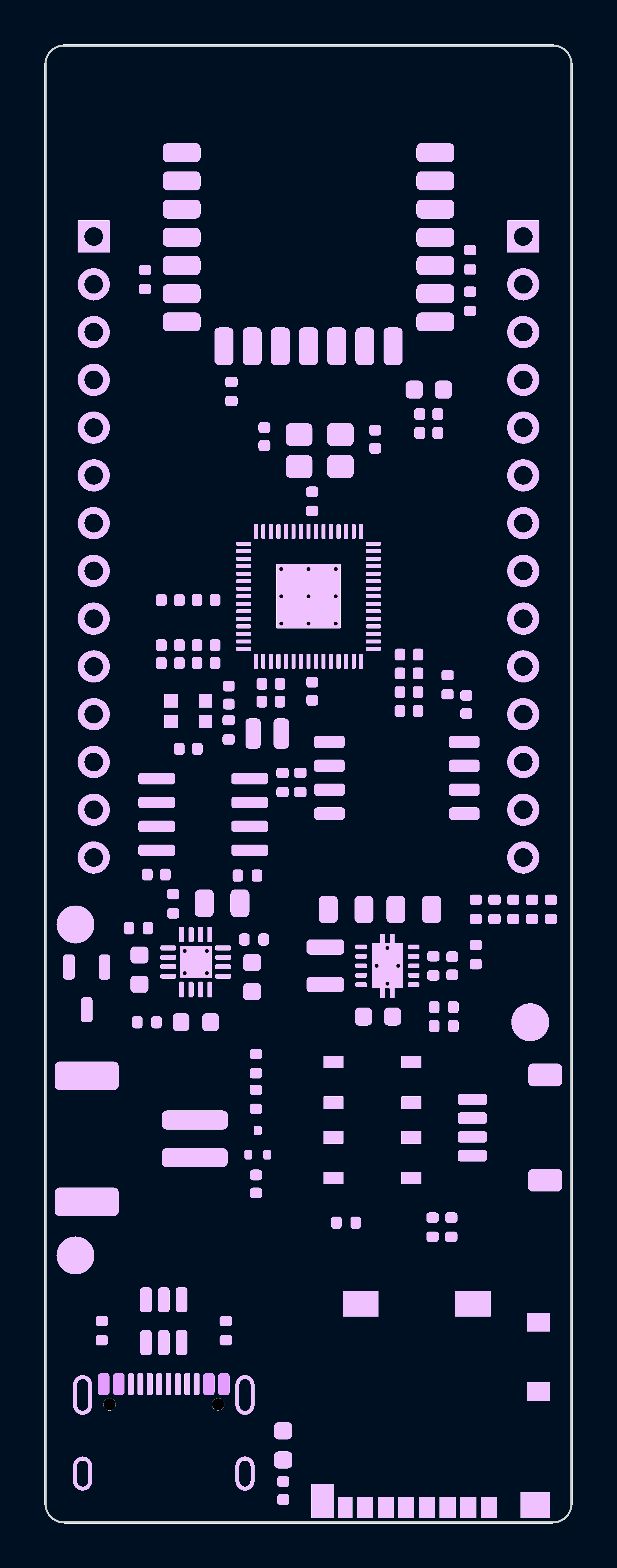
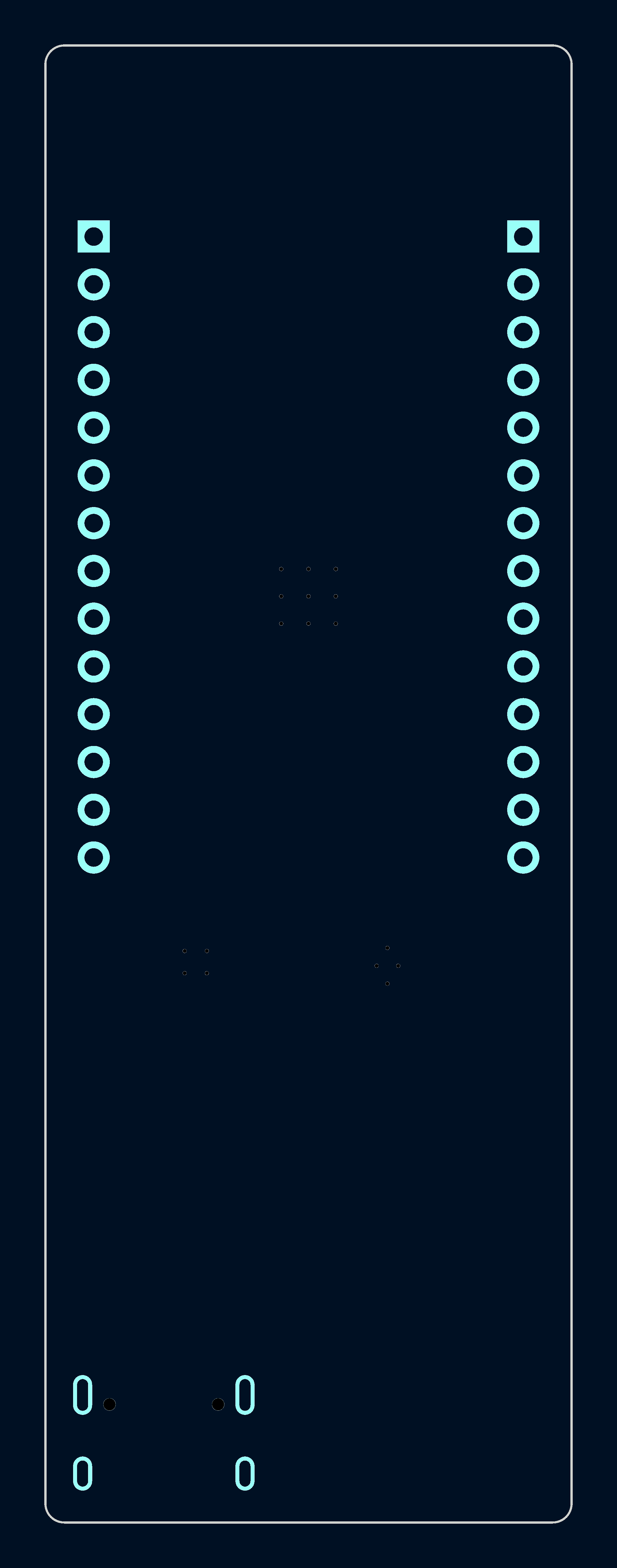
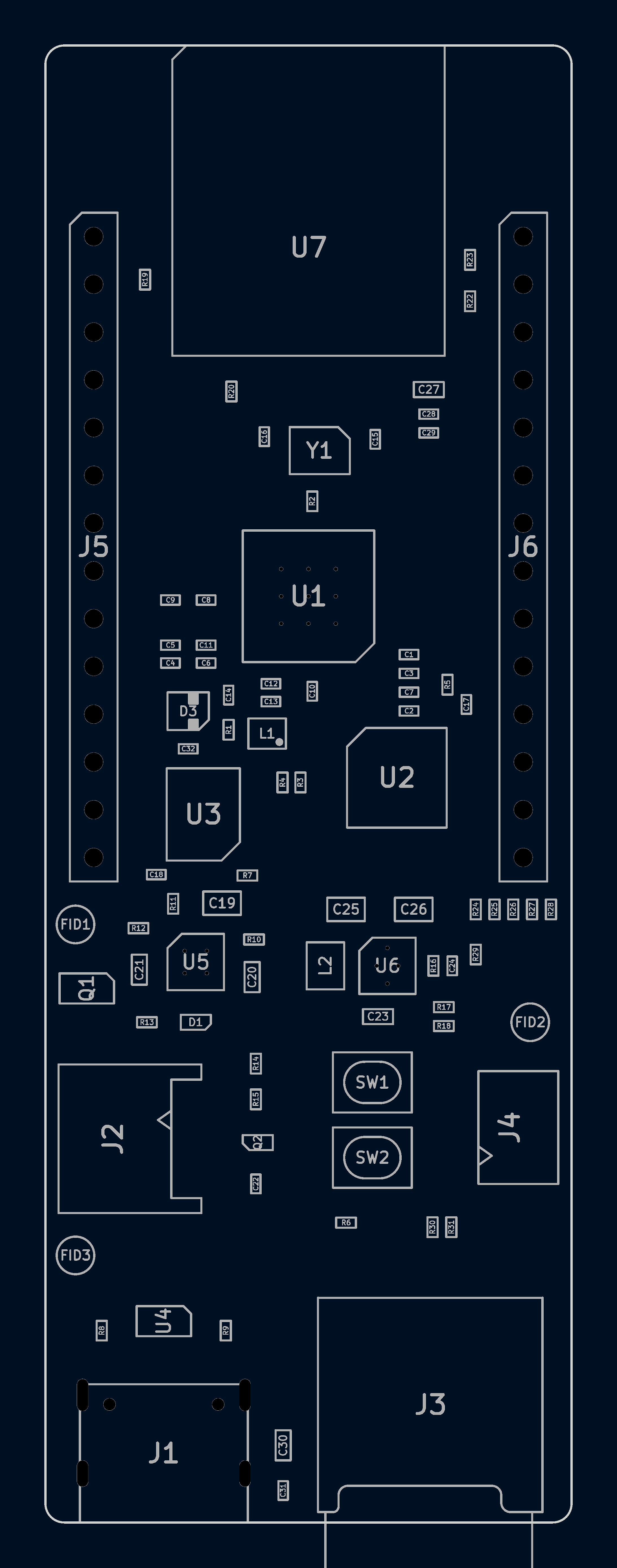
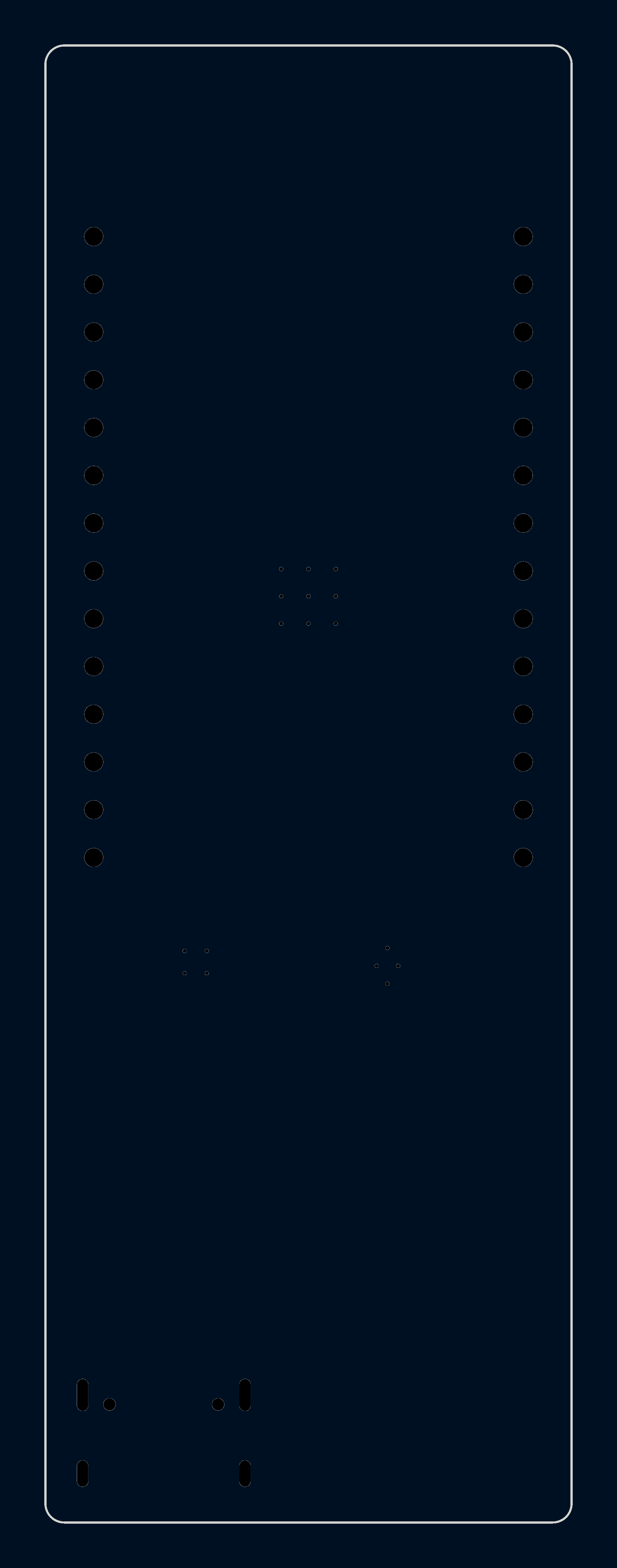
Rendered by kicad-cli with the run's own KiCad version. Dimensions in mm. The layers are the plots the AI judge saw, seen from the top, with their white background made dark. Click one to open it at full size.
- AI cost
- $53.31
- Time
- 4 h 51 min
- Tokens, incl. cache reads
- 90.1M
- 1 board
- $282.37
- 5 boards, per board
- $73.36
- Board size
- 28 × 78.54 mm
- Machine
- EC2 Ubuntu (c7i.2xlarge)
- sprocket
- sprocket 0.5.1
- kicadConnector
- v0.2.0
- kicad
- 10.99.0-6344-g8c85ac1452
Score
Design review9 of 20
- Layout9 of 101 minus 0.1 per minor and 0.2 per major layout finding, down to 0
- Routing0 of 10the same, for routing findings
Circuit checks18.2 of 20
- Decoupling3.2 of 5RP2350 power pins with a capacitor within 3.2 mm
- USB protection5 of 50.5 for an ESD part on D+ and D−, plus 0.25 for each line with a series resistor
- Antenna keepout5 of 51 when there are keepouts and no copper is in them
- Battery drain5 of 51 at 5 µA or less drawn by unswitched battery dividers, falling linearly to 0 at 25 µA
Layout checks24.1 of 30
- Thermal pads9.3 of 10mean over the exposed pads of their vias over the number needed, 0 for a pad with no plane on another layer
- Grounding5.9 of 10USB, QSPI and microSD track length over a ground plane on the next layer
- Silkscreen5 of 5texts at least 0.8 mm high
- Board size3.9 of 51 at the Feather RP2350's 50.8 × 22.8 mm area or less, falling linearly to 0 at 5 times that area
Orderable20 of 20
- Fab notes5 of 51 when every fab option in the notes can be ordered from PCBWay
- Board5 of 51 when the board needs no rework
- BOM lines10 of 101 minus 0.2 for each BOM line that needs a fix, down to 0
Parts data9.9 of 10
- 3D models4.9 of 5parts with a 3D model
- Supplier part numbers5 of 5BOM lines with a valid number from at least one supplier
| The five groups | 81.2 |
|---|---|
| Every gate passed, so no penalty | 0 |
| Score | 81.2 of 100 |
Gates
A board that fails a gate loses 20 points. The gates are the three checks below, every prompt feature, and any fatal review finding.
| Check | Result | What the check found |
|---|---|---|
| Crystal and load capacitors | Pass | Y1 ABM8-272-T3 (CL 10 pF) between XIN and XOUT via R2 1 kΩ; load caps /MCU/XIN: C15 15 pF; /MCU/XOUT_X: C16 15 pF; needs 10.5–17.5 pF per side for 3 pF stray |
| BOOTSEL and RUN buttons | Pass | QSPI_SS (QSPI_SS) → R5 → SW1 → GND; RUN (RUN) → SW2 → GND |
| Charger power path | Pass | U5 BQ24074RGTR: U5 IN (VBUS) is on J1 VBUS; BAT (VBAT) goes to J2; U6 TPS63001DRCR makes +3V3 from OUT (VSYS) |
Prompt features
- Found RP2350 U1
- Found QSPI flash U2
- Found PSRAM U3
- Found USB-C J1
- Found Wi-Fi and BLE U7
- Found microSD J3
- Found Qwiic J4
- Found RGB LED D3
- Found Power-path charger U5
- Found Battery monitoring R14
Design review 9 of 20
Opus 5.5 reviewed an anonymous copy of the board and listed 7 findings. Layout and routing each start at 10 points.
Major
Routing
QSPI_SD3 detours across the board. The flash's IO3 pin is 9.3 mm from the RP2350, but the copper path to it is 65.5 mm long with 8 vias. It daisy-chains through the PSRAM, runs out to the left edge, then crosses under SW1 and comes back up the right side.
Evidence
U1 pad 55 (114.8, 82.74) to U2 pad 7 (122.29, 88.3): 65.5 mm of copper against a 9.3 mm straight line. The path takes vias at (115.0, 84.3), (109.5, 90.9), (105.5, 91.7), (103.6, 91.6), (103.6, 94.2), (122.5, 104.7), (123.8, 103.4) and (124.1, 88.9). It also runs a B.Cu segment from (109.8, 105.2) to (119.8, 105.2) under SW1. The other QSPI lines to U2 are 6.5 to 16.9 mm long.
SD_CLK and SD_D3 detour down the far left edge of the board, although the microSD socket is at the bottom right. The other SD lines run down the right side. This makes the SD clock 87 mm long and D3 98 mm long, each with 5 to 7 vias.
Evidence
SD_CLK from U1 pad 14 (117.45, 76.89) to J3 pad 5 (119.2, 127.74): 87.0 mm against 50.9 mm direct, with 5 vias. It crosses In2.Cu from (118.5, 73.5) to (105.8, 75.9), then runs on B.Cu along x = 104.4 and x = 101.4 from y = 77.3 to 109.9. SD_D3 from U1 pad 19 (115.6, 75.84) to J3 pad 2 (122.5, 127.74): 97.6 mm against 52.4 mm direct, with 7 vias. It runs along In2.Cu at y = 69.1 from x = 114.7 to 101.8, then along F.Cu at x = 101.3 from y = 69.7 to 93.5. For comparison, SD_D0 is 64.5 mm, SD_D1 70.8 mm and SD_D2 74.3 mm.
All of the battery current between the charger's BAT pins and the battery FET necks down to a 0.15 mm track, which is far too narrow for 1.5 A. The rest of the path continues on In2.Cu at 0.4 mm, which is also undersized on an inner layer.
Evidence
U5 pads 2 and 3 (106.54, 98.49 and 98.99) are joined by a 0.25 mm F.Cu track. They reach the via at (105.7, 99.0) only through a 0.15 mm F.Cu segment from (106.4, 99.1) to (105.8, 99.1); check_weird reports it as a narrow-pad-joint. From that via the path to Q1 pad 2 (101.25, 99.0) runs on In2.Cu at 0.4 mm, from (105.6, 99.0) to (103.1, 100.2). The VBAT net class width is 0.4 mm, and the stackup has 35 µm copper on every layer.
USB D+ from contact A6 loops about 18 mm under the USB-C receptacle before joining the B6 branch at the ESD diode. A6 sits 1 mm from B6. The loop leaves D+ uncoupled from D− and forms an 18 mm stub whenever the plug is in the B6 orientation.
Evidence
J1 pad A6 (106.05, 121.18) to U4 pad 6 (107.25, 118.98) is 18.1 mm on F.Cu, routed down to y ≈ 122.7, across to x ≈ 111.6 and back up. J1 pad B6 (107.05, 121.18) to U4 pad 6 is 1.7 mm. D− joins A7 and B7 within 2.4 mm. The total D+ length is 54.5 mm from A6 and 44.4 mm from B6, against 42.4 mm for D−.
Minor
Layout
The charger and the 3.3 V regulator sit in the middle of the board, about 24 mm from the USB-C power input. VBUS has to cross half the board with 7 vias.
Evidence
J1 is at (106.3, 124.86) with its VBUS pads at y = 121.18. U5 is at (108.0, 98.74) and U6 at (118.2, 98.94). VBUS from J1 pad A4 to U5 pad 13 (108.75, 97.28) is 34.1 mm, with 7 vias: (103.9, 121.2), (106.3, 119.0), (108.7, 121.2), (108.8, 115.5), (105.3, 106.0), (110.1, 102.0) and (108.9, 97.3). Part of that run is on In2.Cu.
Routing
Three more QSPI lines take indirect routes with several vias. QSPI_SS loops below the flash before reaching U2 pin 1, QSPI_SD0 to the PSRAM drops to y = 94 first, and PSRAM_CS goes over the top of U1 past the crystal.
Evidence
QSPI_SS from U1 pad 60 (116.8, 82.74) to U2 pad 1 (115.11, 87.03): 20.8 mm and 4 vias, at (117.4, 83.4), (117.6, 87.1), (112.9, 91.6) and (115.0, 87.1), against 4.6 mm direct. QSPI_SD0 from U1 pad 57 to U3 pad 5 (105.93, 88.98): 27.9 mm against 11.5 mm, through vias (114.3, 94.0) and (105.1, 88.9). PSRAM_CS from U1 pad 12 (117.45, 77.69) to U3 pad 1 (110.88, 92.8): 39.1 mm and 4 vias, at (118.4, 71.3), (115.0, 74.3), (106.1, 87.0) and (111.1, 92.5), against 16.5 mm direct.
The USB pair zigzags down through the power stage. D+ passes 0.23 mm from the switch-node pad of the buck-boost inductor.
Evidence
The USB_DP segment from (113.575, 99.13) to (113.575, 99.57) on F.Cu is 0.225 mm edge to edge from L2 pad 1 (BB_L1, 114.9, 99.94). From U4 to R3 and R4 the pair is 37.3 mm long against 27.7 mm direct, zigzagging between x = 111.7 and 114.2 from y = 91 to 111.
Opus 5.5's notes
I wrote review.json with 7 findings: 4 major and 3 minor. None are fatal, so I filed nothing under other.
The upgrade made no changes. kicad-cli pcb upgrade and sch upgrade reported every file as already in the connector's 10.99 format (board 20261031, schematics 20261106). Running the upgrade created a board.kicad_prl settings file, which I deleted, so the design files are byte-for-byte untouched.
| # | Area | Severity | Finding |
|---|---|---|---|
| 1 | routing | major | QSPI_SD3 from U1 pin 55 to U2 pin 7 is 65.5 mm with 8 vias, against 9.3 mm direct. It loops out to the left edge and back under SW1. |
| 2 | routing | minor | QSPI_SS (20.8 mm and 4 vias, against 4.6 mm direct), QSPI_SD0 to the PSRAM and PSRAM_CS all take indirect routes. |
| 3 | routing | major | SD_CLK (87 mm) and SD_D3 (98 mm) run down the far left edge, although the microSD socket is at the bottom right. |
| 4 | routing | major | The battery current from U5's BAT pins passes through a 0.15 mm track at (106.4, 99.1) to (105.8, 99.1), then 0.4 mm on an inner layer. That is too narrow for 1.5 A. |
| 5 | routing | major | USB D+ from J1 contact A6 loops 18 mm under the receptacle before joining B6, which leaves an 18 mm stub in one plug orientation. |
| 6 | routing | minor | The USB pair zigzags through the power stage, and D+ passes 0.23 mm from the switch-node pad of the buck-boost inductor L2. |
| 7 | layout | minor | The charger U5 and the 3.3 V regulator U6 sit about 24 mm from the USB-C connector, so VBUS runs 34 mm with 7 vias. |
Checked with no findings:
- Placement:
- The flash, PSRAM and crystal are 4 to 9 mm from their pins. Those traces are short and have no vias.
- The USB-C, battery, Qwiic and microSD connectors all open off a board edge. The microSD card sticks out 3.45 mm past the bottom edge, which is how Molex draws it.
- The Wi-Fi module's antenna end is flush with the top edge, and no copper or parts sit in front of it.
- Copper: DRC finds no unconnected items, and the copper-hygiene check finds no stubs.
- Pins and footprints: three subagents checked these against the manufacturer datasheets and found no fatal faults. This covered:
- every chip pin mapping, the charger mode straps, and both battery MOSFETs;
- the pin order of the LED, USB-C, microSD and Qwiic connectors;
- every custom footprint.
Left out:
- SW1 and SW2 sit about 8 mm inside the right edge. They are top-pressed buttons a user can still reach, so I didn't report them.
VSYSleaves the charger's OUT pins on 0.25 mm track for about 1 mm. That is a neck-down at the 0.5 mm-pitch pins, so I didn't report it either.
My working files are in scratch/ inside this folder: the extracted netlist, pad and track dumps, the path scripts, plots and the subagents' notes. Delete it if you only want review.json.
Subagent report 1
Task: If you spawn subagents, every `spawn_subagent` call must set `model` to opus-5.5 and `reasoning` to high. Put this same rule, word for word, in every subagent's prompt.
I found no fatal, major or minor problems with U7 (RM2). I checked the footprint, every pin net, the host wiring and the antenna placement against the official RM2 datasheet, release 7 dated 20/02/2026: https://datasheets.raspberrypi.com/rm2/rm2-datasheet.pdf
Confirmed problems
None.
Checked and correct
1. Footprint vs datasheet Fig. 4 (p.7), Fig. 6 (p.9) and Fig. 7 (p.10)
The footprint is not mirrored or rotated, and it is on F.Cu.
| Item | Datasheet | RMC20452T.kicad_mod / board |
|---|---|---|
| Module body | 14.5 × 16.5 mm | F.Fab ±7.25 × ±8.25 mm, so the absolute body is x 106.75–121.25, y 50.00–66.50 |
| Pads | 21 castellated pads, 1.0 × 2.0 mm, 1.5 mm pitch, 0.5 mm overhang past the body edge | 2.0 × 1.0 mm, 1.5 mm pitch, centres 0.5 mm inside the edge, so 0.5 mm sticks out |
| Side pins 7 and 15 | 1.8 mm from the bottom edge | y = +6.45, which is 1.8 mm from +8.25 |
| Bottom pins 8 and 14 | 2.75 mm from the side edges | x = ±4.5 |
| Numbering (top view) | Pin 1 top-left, counter-clockwise: 1–7 down the left, 8–14 along the bottom, 15–21 up the right | Pads 1–7 at x −6.75 going downward (abs 107.25, y 55.7→64.7); 8–14 at y +7.75 left to right (abs y 66.0, x 109.5→118.5); 15–21 at x +6.75 going upward. Pin 1 is at the top-left (107.25, 55.70) |
| Antenna end | Above pins 1 and 21 | Toward −y |
| RF keepout | 35.5 mm wide, 13.5 mm past the module top, ending 5.0 mm below the module top | Zone ±17.75 × (−21.75…−3.25), all copper layers. Absolute 96.25–131.75 × 36.5–55.0 |
The board file uses the new (transform (translate 114 58.25)) format, so the keepout coordinates stored inside the footprint are relative. The keepout therefore sits on the part, not off the board.
2. Pin nets vs Table 2 (p.10), Table 1 in §1.3.2 (p.5) and §2.6 (p.11)
| Pin | Function | Net | Matches |
|---|---|---|---|
| 1, 4, 7, 11, 15, 21 | GND | GND | ✓ |
| 2, 19, 20 | NC | unconnected | ✓ |
| 3 | gSPI SCLK | WL_CLK → U1.43 GPIO29 | ✓ |
| 5 | gSPI DI | WL_D → U1.36 GPIO24 | ✓ |
| 6 | gSPI DO | R19 470 Ω → WL_D | ✓ (470 Ω per Table 1) |
| 9 | gSPI CS | WL_CS → U1.37 GPIO25 | ✓ |
| 10 | nIRQ | R20 10 kΩ → WL_D | ✓ (10 kΩ per Table 1) |
| 12 / 13 | WL_ON / BT_ON | both on WL_ON → U1.35 GPIO23 | ✓ |
| 14 | VDDIO (3.3 V or 1.8 V) | +3V3 | ✓ |
| 16 | VIN (3.0–4.8 V; RF performance drops below 3.2 V) | +3V3 from the fixed 3.3 V TPS63001 | ✓ within rating |
| 8 | GPIO0 | unconnected | OK, optional |
| 17 | GPIO2 | VBUS divider, R22 100 kΩ / R23 150 kΩ | ✓ VBUS 5.0 V gives 3.0 V and 5.5 V gives 3.3 V, so it stays ≤ VDDIO. 3.3 V ±5% I/O VIH is 2.0 V (Table 4), so detection threshold ≈ 3.3 V |
| 18 | GPIO1 | PS_SYNC to U6 TPS63001 PS/SYNC, with R18 100 kΩ pulldown | ✓ Same use as Pico 2 W (§1.3.3 GPIO expansion: "SMPS power save") |
I also checked the RP2350A QFN-60 pin numbers against the RP2350 datasheet Fig. 2 (§1.2.1.1): pin 35 is GPIO23, 36 is GPIO24, 37 is GPIO25 and 43 is GPIO29. The symbol pin functions in nets.txt agree with Table 2 for all 21 pins.
3. Placement
U7 sits at (114.0, 58.25), rotation 0. Its antenna end (body top at y = 50.00) is flush with the top board edge at y = 50, so the antenna points out of the board. The board corner arcs are well outside x 106.75–121.25.
Nothing is in front of the antenna, because the area past y = 50 is off the board.
No pad, track, arc or via from any other footprint has y < 57. The nearest parts are:
- J5 pin 1 at (102.57, 60.16)
- J6 pin 1 at (125.43, 60.16)
- R23 at (122.6, 61.4)
All three sit beside the module body, behind the keepout's lower edge at y = 55.0.
No copper zone fill on any layer overlaps the RF keepout region. I checked this with shapely intersections of every zone fill against the keepout.
Scratch files, including the datasheet page renders and the U7 area render, are in /home/ubuntu/review/scratch/sub_wireless/.
Subagent report 2
Task: If you spawn subagents, every `spawn_subagent` call must set `model` to opus-5.5 and `reasoning` to high. Put this same rule, word for word, in every subagent's prompt.
I found no fatal fault in any of the nine footprints. Every pad map, pin‑1 location, pitch and connector opening matches the manufacturer drawing.
I compared each library footprint pad by pad with the stock KiCad 10 footprint of the same name. D3, J2, J3, U5 and U6 have identical pads. L1 has the same pads plus a polarity dot. J1 and J4 are the stock footprints. I then checked the footprints against the manufacturer drawings below. Scratch renders and PDFs are in scratch/sub_fp/.
Confirmed problems
None at minor, major or fatal level.
Checked and correct
| Ref | Checked | Evidence |
|---|---|---|
| D3 WS2812B‑2020‑V6 | The pads are 0.7×0.7 mm at ±0.915/±0.55. That matches the 0.7 mm pads, 0.40 mm gap and 1.13 mm inner spacing. Rotating the datasheet top view by 180° gives the footprint order 1 DO top‑left, 2 GND bottom‑left, 3 DI bottom‑right, 4 VDD top‑right. Board pads: 1 (108.515,85.95) unconnected DOUT, 2 (108.515,84.85) GND, 3 (106.685,84.85) RGB_DIN, 4 (106.685,85.95) +3V3. VDD at 3.3 V is within the V6 range of 3.3–5.3 V. | Worldsemi WS2812B‑2020‑V6 datasheet p.2, "PCB Solder Pad" and "Pin Arrangement": https://file.thegioiic.com/upload/documents/1792377585_WS2812B-2020-V6.pdf |
| J2 S2B‑PH‑SM4‑TB | Signal pads are 1.0×3.5 mm at 2.0 mm pitch. The MP pads are 1.5×3.4 mm. The body outline is 7.9 mm wide by 6.0 mm deep, matching B = 7.9 and depth 6. Pin 1 is on the left when you look into the opening, as the drawing shows. The signal pads sit at x=107.95, so the opening faces −x. The front face is at x≈100.7, 0.7 mm inside the left edge. The cable enters from off the board. | JST ePH.pdf p.4, "Side entry type": https://www.jst-mfg.com/product/pdf/eng/ePH.pdf |
| J3 Molex 104031‑0811 | All 14 pads match the "Recommended PCB layout" rotated 180°. Details are below the table. | Molex SD‑104031‑001 sheet 1 (copy at https://www.limpulsion.fr/upload/docs/1040310811.PDF; Molex's own server timed out) |
| J4 SM04B‑SRSS‑TB (stock) | The signal pads sit at x=122.72 and the MP pads at x=126.595. The body front is at x≈127.3, 0.7 mm inside the right edge, so the cable enters from the right edge. The pin order is 1 GND, 2 +3V3, 3 SDA, 4 SCL, which is the Qwiic order. | Stock footprint, after JST eSH.pdf |
| J1 USB4105‑GF‑A (stock) | The footprint's "PCB Edge" line is at local y=+3.675, which lands on board y=128.54, the bottom edge exactly. That fits the drawing: the front slot centre is 2.60 mm from the PCB edge, and the board has 128.54−125.94 = 2.60. The shell front is flush with the edge and the opening faces off the board. The pins carry the right nets: CC1 on A5, CC2 on B5, D+ on A6/B6, D− on A7/B7, VBUS on A4/A9/B4/B9 and GND on A1/A12/B1/B12. | GCT USB4105 drawing, "Recommended PCB Layout": https://gct.co/files/drawings/usb4105.pdf |
| L2 DFE252012F | The pads are 0.8×2.0 mm at ±1.0. That is exactly Murata's pattern of 1.2 mm gap, 2.8 mm overall and 2.0 mm height. | Murata datasheet, "Recommended patterns": https://www.murata.com/~/media/webrenewal/products/inductor/chip/tokoproducts/wirewoundmetalalloychiptype/m_dfe252012f.ashx |
| L1 AOTA‑B201610S3R3‑101‑T | It solders and assembles. The pads are KiCad's stock 0.8×1.6 mm at ±0.75, which is smaller than Abracon's 1.0×1.6 mm pads with a 1.0 mm gap. They still cover the 0.6 mm terminals at 0.4–1.0 mm from centre, so I don't report this. The polarity dot sits at pad 1, which is on +1V1, and pad 2 is on VREG_LX. That matches the RP2350 datasheet Fig. 26, where the orientation indicator is on the V<sub>OUT</sub> end. | Abracon datasheet p.4: https://abracon.com/datasheets/AOTA-B201610S3R3-101-T.pdf; RP2350 datasheet §6.3.8, Figs. 26 and 28 (scratch/rp2350.pdf p.412–414) |
| U5 BQ24074 RGT0016C | The pitch is 0.5 mm and pad centres span 2.8 mm. The 0.825×0.25 mm pads are slightly longer than TI's 0.6×0.24 mm. The thermal pad is 1.68 mm with vias at ±0.59, against TI's ±0.58. Pin 1 is top‑left and the numbering runs counter‑clockwise. Every pin carries its datasheet function. | TI SLUS810N Fig. 7‑2, p.7, and RGT0016C land pattern, p.53: https://www.ti.com/lit/ds/symlink/bq24074.pdf |
| U6 TPS63001 DRC0010J | The pads are 0.6×0.24 mm at ±1.4 with 0.5 mm pitch. The exposed pad is 1.65×2.4 mm with tabs out to 3.4 mm, and the vias sit at (0,±0.95) and (±0.575,0). Pin 1 is top‑left, 1–5 run down the left side and 6–10 up the right. Every pin carries its datasheet function, and FB is tied to +3V3 as the fixed‑output version needs. | TI SLVS520C, Pin Configuration p.3 and DRC0010J land pattern p.24: https://www.ti.com/lit/ds/symlink/tps63001.pdf |
J3 microSD details
- Pads:
- Pin 1 centre is 3.105 mm from the socket centre, on the detect‑switch side.
- Pin 8 is the narrow 0.75 mm pad.
- The ground pads G1–G4 are 1.55, 1.17, 1.9 and 1.9 mm wide.
- The detect pads are 1.2×1.0 mm, 6.15 and 9.85 mm from the pin row.
- Pin map: it matches the drawing's table (T1 DAT2, T2 CD/DAT3, T3 CMD, T4 VDD, T5 CLK, T6 Vss, T7 DAT0, T8 DAT1). The board nets follow it: SD_D2, SD_D3, SD_CMD, +3V3, SD_CLK, GND, SD_D0, SD_D1. Pads 9 and 10 form the detect switch, on SD_DET and GND.
- Card entry: the card goes in on the same side as the pin tails. Molex lists "Card Entry Location: Front", and the drawing's card outline sticks out 4.0 mm past the tail side. On the board the tails are at y=127.74, the body front is at y≈127.99 and the bottom edge is at 128.54. So the slot opens off the bottom edge, and an inserted card sticks out about 3.45 mm past the edge.
- 3D model: the model is rotated 180° compared with the stock footprint. It is a different STEP file, and
renders/top.pngshows its tails over the pad row, so the rotation only lines the model up with the pads.
Other things checked
- Copper near the bottom edge: J3's pin and shell pads end at y=128.29. That is 0.25 mm from the edge and about 0.30 mm from the corner arc, which meets the project's 0.25 mm
min_copper_edge_clearance. - Battery wiring on J2: pin 1 is GND and pin 2 is BAT_CONN. The footprint matches the drawing. Whether a given LiPo pack's leads match this order is a battery choice I did not check.
Subagent report 3
Task: If you spawn subagents, every `spawn_subagent` call must set `model` to opus-5.5 and `reasoning` to high. Put this same rule, word for word, in every subagent's prompt.
I found no confirmed fatal faults in the parts you assigned. Every pin number matched the manufacturer's datasheet, and every strap and power path works. No files were changed.
Confirmed fatal problems None.
Checked and correct
- U5 BQ24074 pins match TI SLUS810 (https://www.ti.com/lit/ds/symlink/bq24074.pdf), Fig. 7-2 and Table 7-1: 1 TS, 2/3 BAT, 4 CE, 5 EN2, 6 EN1, 7 PGOOD, 8 VSS, 9 CHG, 10/11 OUT, 12 ILIM, 13 IN, 14 TMR, 15 ITERM, 16 ISET, 17 pad to VSS. On the BQ24074, pin 15 is ITERM, not SYSOFF (SYSOFF is only on the '75 and '79).
- U5 straps:
- CE is tied to GND, so charging is enabled.
- EN2 = 0 and EN1 = 1 (tied to OUT) selects USB500 mode (Table 7-2). Both EN pins are driven, not left floating.
- TS has a fixed 10 kΩ (R12) to VSS, which the datasheet allows when the battery has no NTC.
- TMR open gives the default timers. ITERM open gives the default 10% termination.
- U5 values and limits:
- R11 2 kΩ gives about 445 mA charge current (KISET 890 AΩ, allowed 590 Ω to 8.9 kΩ).
- R10 1.74 kΩ is in the allowed 1.1 to 8 kΩ range.
- The highest voltage on EN1 is OUT at 4.5 V, under the 7 V abs-max. IN is rated to 28 V.
- U6 TPS63001 pins match TI (https://www.ti.com/lit/ds/symlink/tps63001.pdf), Pin Functions table: 1 VOUT, 2 L2, 3 PGND, 4 L1, 5 VIN, 6 EN, 7 PS/SYNC, 8 VINA, 9 GND, 10 FB, 11 pad to PGND.
- FB is tied to VOUT, as the fixed-output version requires.
- EN is pulled to VSYS through R17 100k. PS/SYNC is pulled down by R18, so it starts in power-save mode.
- VINA has the R16 100 Ω / C24 filter. VSYS stays at or below 4.5 V, inside the 5.5 V input limit.
- Q1 DMG2305UX (https://www.diodes.com/assets/Datasheets/DMG2305UX.pdf): the SOT-23 pins are 1 G, 2 S, 3 D, matching the nets (gate GND, source VBAT, drain BAT_CONN).
- With the battery correct, the body diode conducts from drain to source. That gives Vgs of about −VBAT, well past the −0.9 V max threshold, so the FET turns fully on. It then carries current both ways, so the battery can power the board and be charged.
- With the battery reversed and no USB, the FET stays off. Vgs stays within the ±8 V rating.
- Q2 DMG1012T (https://www.diodes.com/assets/Datasheets/DMG1012T.pdf): the SOT-523 pins are 1 G, 2 S, 3 D, matching the nets.
- The divider point is at most 2.1 V. With the gate at 3.3 V, Vgs is at least 1.2 V, above the 1.0 V max threshold, so the FET passes the voltage to the ADC.
- When 3V3 is off, the FET is off and its body diode (ADC side to divider) is reverse-biased, so the GPIO28 pin is isolated from the battery.
- U4 USBLC6-2SC6 (https://www.st.com/resource/en/datasheet/usblc6-2.pdf), functional diagram: 1/6 I/O1 on USB_DP, 3/4 I/O2 on USB_DM, 2 GND, 5 VBUS. All match.
- U2 W25Q128JV (Winbond datasheet, §3.3, SOIC 208-mil): 1 /CS, 2 IO1, 3 IO2, 4 GND, 5 IO0, 6 CLK, 7 IO3, 8 VCC. These match the QSPI nets.
- U3 APS6404L (https://www.pjrc.com/store/APS6404L_3SQR.pdf, §3.1): 1 CE#, 2 SIO1, 3 SIO2, 4 VSS, 5 SIO0, 6 SCLK, 7 SIO3, 8 VDD. These match. The -3SQR part runs from 2.7 to 3.6 V.
- GPIO8 as PSRAM chip select: the RP2350 datasheet GPIO function table lists F9 "QMI CS1n" on GPIO 0, 8, 19 and 47. The FLASH_DEVINFO CS1_GPIO field also allows 0, 8, 19 and 47. R7 pulls the line up.
- J1 USB-C uses the standard pin names:
- CC1 (A5) and CC2 (B5) each have a separate 5.1k pull-down.
- VBUS is on A4, A9, B4 and B9. GND is on A1, A12, B1 and B12.
- D+ is on A6 and B6, D− on A7 and B7, so both plug orientations work.
- J3 microSD (Molex 104031-0811 drawing): contacts 1 DAT2, 2 CD/DAT3, 3 CMD, 4 VDD, 5 CLK, 6 VSS, 7 DAT0, 8 DAT1 match the nets.
- The card-detect switch is open with no card and closes when a card is inserted. One side goes to GND (pin 10) and the other to SD_DET, which R29 pulls up to 3V3 (pin 9). That works whichever way the two switch pins are assigned.
- The SD bus fits PIO SDIO: D0 to D3 sit on consecutive GPIOs 12 to 15, and CLK on GPIO10 is D0−2, the usual offset.
- D3 WS2812B-2020-V6 (Worldsemi V6 sheet): 1 DOUT, 2 GND, 3 DIN, 4 VDD match the nets. The V6 is rated from 3.3 V.
- J4 Qwiic: 1 GND, 2 3V3, 3 SDA (GPIO4), 4 SCL (GPIO5) matches SparkFun's order, with 2.2k pull-ups R30 and R31. GPIO4 and GPIO5 are I2C0 SDA and SCL.
- Power-on orders: USB only, battery only and both all reach 3V3 correctly. The BQ24074 blocks current flowing back from BAT or OUT into IN. Pulling 3V3_EN low just turns off the TPS63001 and isolates Q2. Feeding 5 V into J6.2 only reaches IN and the USBLC6, which is fine.
Non-fatal observations
- R10 (ILIM) has no effect in this strap: EN2 = 0 and EN1 = 1 means the input is capped at 500 mA. The ILIM resistor only applies when EN2 = 1 and EN1 = 0.
- 5 V fed into J6.2 while a USB host is plugged in pushes current back into the host's VBUS, because there is no diode.
- With USB connected and the battery plugged in backwards, the charger's BAT voltage turns Q1 on. The protection only works when no USB is present.
- The WL_VBUS_DET divider puts about 3.0 V into the RM2's GPIO2 even when the RM2 is unpowered, but the 100k limits the current to about 30 µA or less.
- The R14/R15 divider draws about 4.5 µA from the battery all the time.
- Erratum RP2350-E14: the bootrom's
connect_internal_flash()sets up the pads for pin 0 rather than GPIO8. The workaround is in firmware: clear GPIO8's pad isolation after that call.
Circuit checks 18.2 of 20
Decoupling
3.2 of 59 of 14 RP2350 power pins have a capacitor within 3.2 mm.
| Pin | Pad | Net | Nearest capacitor | Distance |
|---|---|---|---|---|
| IOVDD | 1 | +3V3 | C1 | 1.45 mm |
| DVDD | 6 | +1V1 | C7 | 4.53 mm |
| IOVDD | 11 | +3V3 | C1 | 4.53 mm |
| IOVDD | 20 | +3V3 | C29 | 7.05 mm |
| DVDD | 23 | +1V1 | C8 | 6.17 mm |
| IOVDD | 30 | +3V3 | C11 | 6.43 mm |
| IOVDD | 38 | +3V3 | C11 | 3.01 mm |
| DVDD | 39 | +1V1 | C8 | 1.53 mm |
| ADC_AVDD | 44 | +3V3 | C11 | 1.53 mm |
| IOVDD | 45 | +3V3 | C11 | 1.53 mm |
| VREG_AVDD | 46 | /MCU/VREG_AVDD | C14 | 1.96 mm |
| VREG_VIN | 49 | +3V3 | C12 | 1.2 mm |
| USB_OTP_VDD | 53 | +3V3 | C10 | 1.14 mm |
| QSPI_IOVDD | 54 | +3V3 | C10 | 1.14 mm |
USB protection
5 of 5- ESD parts on D+ and D−
- U4
- D+ nets, connector to RP2350
- USB_DP → /MCU/USB_DP_MCU series resistor
- D− nets, connector to RP2350
- USB_DM → /MCU/USB_DM_MCU series resistor
Differential pair, not scored
- D+ and D− length
- 66.19 mm and 50.77 mm
- Mismatch
- 15.42 mm
- Vias
- 0
- Longest coupled stretch
- 32.9 mm on F.Cu, 0.2 mm wide, 0.15 mm gap
- Differential impedance
- 100.3 Ω
Antenna keepout
5 of 51 keepout covers the Wi-Fi module U7.
| Keepout | Layers | Copper inside |
|---|---|---|
| U7 footprint | F.Cu, B.Cu, In1.Cu, In2.Cu | none |
Battery drain
5 of 5Unswitched dividers draw 4.47 µA from a full battery, even when the board is off.
| Divider | Buffered by | Switched by | At 4.2 V |
|---|---|---|---|
| R14 470k / R15 470k | none | none | 4.47 µA |
Layout checks 24.1 of 30
Thermal pads
9.3 of 10| Exposed pad | Net | Vias | Needed | Plane on another layer |
|---|---|---|---|---|
| U1 | GND | 9 | 9 | yes |
| U5 | GND | 4 | 5 | yes |
| U6 | GND | 4 | 4 | yes |
Grounding
5.9 of 10| Bus | Over ground | Track length | Share |
|---|---|---|---|
| USB | 117 mm | 117 mm | 100% |
| QSPI | 80.5 mm | 178.2 mm | 45.2% |
| microSD | 306.5 mm | 559.9 mm | 54.7% |
| All three | 504 mm | 855.1 mm | 58.9% |
Silkscreen
5 of 50 of 30 texts are below PCBWay's 0.8 mm minimum. The smallest is 0.9 mm.
Board size
3.9 of 528 × 78.54 mm, 2199 mm². The Feather RP2350 is 50.8 × 22.8 mm.
Orderable 20 of 20
| 1 board | 5 boards | |
|---|---|---|
| PCBs | $156.77 | $156.77 |
| Assembly | $88.00 | $88.00 |
| Components | $37.60 | $122.01 |
| Total | $282.37 | $366.78 |
| Per board | $282.37 | $73.36 |
PCBWay's instant quote for the options in the fab notes, without shipping. PCBWay makes at least 5 PCBs, so 1 board is 5 PCBs with 1 assembled. Parts are at distributor list prices.
Fab notes
5 of 5No fixes needed.
Board
5 of 5No fixes needed.
BOM lines
10 of 100 of 38 BOM lines need a fix.
Parts data 9.9 of 10
3D models
4.9 of 51 part has no 3D model the run's KiCad can load: Q2.
Supplier part numbers
5 of 538 of 38 BOM lines have a valid supplier part number.
LCSC 100%, Digi-Key 0%, Mouser 0%
Stock
100% of 40 BOM lines are stocked for 5 boards at LCSC, JLCPCB or Digi-Key.
| Parts | MPN | At |
|---|---|---|
| C25,C26 | CL21A226MAQNNNE | Digi-Key |
DRC and ERC
| Errors | Warnings | Unconnected | |
|---|---|---|---|
| DRC | 0 | 0 | 0 |
| ERC | 0 | 0 |
DRC by type: lib_footprint_mismatch 1. Footprints that differ from their library copy aren't counted as warnings.
Files
The agent's README
RP2350 dev board
A 28 × 78.54 mm, 4-layer RP2350A board with Wi-Fi/BLE, a LiPo charger and microSD, laid out for PCBWay's standard PCB and turnkey assembly service. Every fitted part is on the top side.
| Block | Part | Notes |
|---|---|---|
| MCU | RP2350A (U1), 12 MHz crystal | Core supply from the internal switching regulator (L1 3.3 µH) |
| Flash | W25Q128JVSIQ (U2), 16 MB | QSPI CS0, boots from it |
| PSRAM | APS6404L-3SQR-SN (U3), 8 MB | QSPI CS1 on GPIO8 |
| USB | USB-C (J1, GCT USB4105), 5.1 kΩ CC pull-downs, USBLC6-2 ESD | USB 2.0 full speed, power and data |
| Charger | BQ24074 (U5) with power path | 445 mA charge current, 500 mA input limit |
| Battery | JST PH 2-pin (J2), reverse-polarity P-FET (Q1) | Single-cell LiPo |
| Battery monitor | 470 k/470 k divider on GPIO28 (ADC2), switched by Q2 | VBAT = 2 × ADC |
| 3.3 V | TPS63001 buck-boost (U6) | Runs from the cell or USB; 3V3_EN on the header turns it off |
| Wireless | Raspberry Pi RM2 module (U7, CYW43439) | Wi-Fi 4 and Bluetooth 5.2, same wiring as the Pico 2 W |
| microSD | Molex 104031-0811 (J3) | 4-bit SD on GPIO10-15, card detect on GPIO9 |
| Qwiic / STEMMA QT | JST SH 4-pin (J4) | I²C0 on GPIO4 (SDA) and GPIO5 (SCL), 2.2 kΩ pull-ups |
| RGB LED | WS2812B-2020 (D3) | Data on GPIO22 |
| Buttons | BOOTSEL (SW1), RESET (SW2) | |
| Headers | 2 × 14 pins on 2.54 mm, rows 22.86 mm apart (J5, J6) | Holes only; not fitted. Pin names on the bottom silkscreen |
Files
| Path | Contents |
|---|---|
rp2350-devboard.kicad_pro |
KiCad project: schematic (5 sheets) and PCB |
BOM.csv |
Bill of materials |
fab/ |
Gerbers, drill files and job file (gerbers/, zipped as rp2350-devboard-gerbers.zip), PCBWay BOM and centroid |
docs/assembly.md |
Assembly and bring-up instructions |
docs/renders/ |
3D renders |
lib/ |
Project symbols, footprints and 3D models |
scripts/ |
Generators: design.py holds every part and net, the other scripts build the schematic and board, finish it (teardrops.py, label_board.py) and export fab/ (export_fab.py) |
The schematic, placement and pre-routed copper come from the scripts. Edit the schematic and board in KiCad now.
build_schematic.py assigns new UUIDs, which breaks the link to the routed board, and build_pcb.py replaces the
routed board.
Pinout
Left header J5, pin 1 at the top (USB-C is at the bottom):
| Pin | 1 | 2 | 3 | 4 | 5 | 6 | 7 | 8 | 9 | 10 | 11 | 12 | 13 | 14 |
|---|---|---|---|---|---|---|---|---|---|---|---|---|---|---|
| J5 | GND | 3V3 | SWCLK | SWDIO | RUN | GP16 | GP17 | GP18 | GP19 | GP20 | GP21 | GP26/A0 | GP27/A1 | GND |
| J6 | GND | VBUS | GND | 3V3 | GP7 | GP6 | GP5/SCL | GP4/SDA | GP3 | GP2 | GP1 | GP0 | GND | 3V3_EN |
Fixed functions:
| GPIO | Function |
|---|---|
| 8 | PSRAM CS |
| 9 | microSD card detect (low when a card is in) |
| 10-15 | microSD CLK, CMD, D0, D1, D2, D3 |
| 22 | WS2812B data |
| 23, 24, 25, 29 | RM2 WL_ON, WL_D, WL_CS, WL_CLK (as on the Pico 2 W) |
| 28 | Battery voltage / 2 |
Design decisions
- Pico 2 W compatible wireless. The RM2 uses GPIO23/24/25/29 and the same 470 Ω/10 kΩ data network, and its
WL_GPIO2 senses VBUS through a 100 k/150 k divider. Stock MicroPython and the Pico SDK
pico2_wboard files drive Wi-Fi and BLE unchanged. - No WL_GPIO0 LED. The Pico 2 W's LED hangs off the RM2. Its track would block the left header fan-out, and the
RGB LED already serves as the user LED, so U7 pin 8 is unconnected.
Pin("LED")on stockpico2_wfirmware runs without error but lights nothing. Use the WS2812B on GPIO22. - Charger in USB500 mode. EN1 is tied high and EN2 low, so the BQ24074 draws at most 500 mA from any USB port without negotiation. ISET = 2 kΩ sets 445 mA fast charge, which suits cells from about 450 mAh up. R10 (ILIM) only matters if EN1/EN2 are changed to resistor-programmed mode.
- Power path. The BQ24074 OUT pin (VSYS) feeds the TPS63001 from USB when present, else from the cell. The buck-boost keeps 3.3 V across the full LiPo range (3.0-4.2 V) and from USB (VSYS = 4.4 V).
- VSYS not on the header. VSYS is tied to the cell through the charger's internal BAT-OUT FET, so 5 V fed there would charge the cell with no regulation. External 5 V power goes in through VBUS (J6 pin 2), which passes the charger's input current limit and over-voltage protection.
- 3V3_EN. Pulled up to VSYS with 100 kΩ. Grounding J6 pin 14 turns off 3.3 V while the charger keeps working.
- Battery monitor back-power blocker. The divider reads VBAT/2, up to 2.1 V. With the 3.3 V rail off, that voltage would forward-bias the GPIO28 clamp diode into an unpowered IOVDD. Q2, an N-FET gated by +3V3, connects the divider to the pin only while 3.3 V is up. The divider draws 4.5 µA from the cell.
- 2.2 kΩ PSRAM CS pull-up. At power-on the RP2350 pulls GPIO8 down (36 kΩ minimum). 2.2 kΩ keeps CE# above the PSRAM's V_IH so it stays deselected until firmware configures CS1.
- Reverse-battery P-FET (Q1). A reversed cell leaves the FET off, so the charger and buck-boost see no negative voltage.
- Headers not fitted. J5/J6 are holes only, so the board can be soldered down, socketed or fitted with headers by the user. J1's four shell tabs are the only plated through-holes that get solder. PCBWay solders them with paste-in-hole or by hand.
Layout
- Stackup: PCBWay standard 1.6 mm 4-layer, 1 oz outer copper, ENIG. F.Cu signals and parts, In1.Cu solid GND with no tracks, In2.Cu +3.3 V plane that also carries signals (see the reviewer notes), B.Cu signals with GND pour.
- Rules: 0.15 mm track and clearance for signals (PCBWay minimum 0.127 mm), 0.6/0.3 mm vias, USB pair 0.2 mm.
- Power copper: VBUS, VSYS, VBAT, BAT_CONN and the inductor nets run at 0.4 mm and +1V1 at 0.2-0.25 mm. The narrowest pieces are 0.15 mm stubs where they enter fine-pitch pins: about 0.7 mm of VBAT at U5's BAT pins and the EN1 tie to VSYS. +3V3 reaches the parts through the In2 plane.
- The RM2 sits at the top edge with its antenna past the copper. Its footprint carries the datasheet's RF keepout on all copper layers. The datasheet forbids metal only in the antenna keepout, so tracks and vias run under the module body.
- The RP2350 regulator follows Raspberry Pi's hardware design guide: VREG_LX runs between the C12 and C13 pads to L1. A custom DRC rule allows that one net 0.127 mm clearance, still at PCBWay's minimum.
- Switch-node keepouts on In2.Cu and B.Cu keep signal tracks out of the fields under the buck-boost (tracks and vias) and the RP2350 regulator (tracks only, so a GND via can drop the C12/C13 return straight to the plane). GND still pours in both.
- Drawn by hand in
scripts/hand_routes.pyandscripts/build_pcb.py: the top-left fan-out (SWD, RUN, GP16-27, VBAT_SENSE, RGB_DIN and the RM2 lines), USB_D±_MCU from U1 to R3/R4, the VREG_LX loop, and the buck-boost BB_L1/BB_L2/VSYS/+3V3 loop. The USB pair was routed as a differential pair and locked before the autoroute. The router did the rest, then GND stitching vias and a 3 mm edge fence went in. - Teardrops on every pad and via. Reference designators are hidden on the silkscreen and shown on F.Fab.
Reviewer notes
- DRC. ERC is clean. DRC has 0 errors, 0 unconnected items and clean schematic parity. One warning remains: R7's top silk line touched U3's pin-1 mark and was deleted, so R7 no longer matches its library footprint.
- Via in pad. The router put 82 vias in or against SMD pads, such as on the decoupling caps, U1, U2, U3 and J1. They are marked filled and capped, so the order needs PCBWay's resin-filled, capped vias, which cost more. Moving them beside the pads by hand would allow plain tented vias.
- In2 is a split plane. About 410 mm of other nets run on In2.Cu: SD bus, RUN, GP4, QSPI_SCLK (23 mm), PSRAM_CS, +1V1, VBUS and others. The +3.3 V copper still connects everywhere, but these traces reference a broken plane on one side. That is fine at the default QSPI clock. Check flash and PSRAM signal quality before raising the QSPI clock.
- Routing quality. The autorouted copper is functional but not tidy. Some routes are long, for example GP0 runs under U2, and a hand cleanup pass would shorten several.
- L1 stock. The Abracon 3.3 µH 0806 inductor had 143 at JLCPCB and 10 at LCSC in November 2026. Any 2016 (0806) 3.3 µH molded inductor rated ≥ 1 A with DCR ≤ 150 mΩ is a drop-in substitute.
- Fiducials. The antenna keepout and the header rows leave no room for fiducials near the top, so the three fiducials sit in the lower half of the board. They still form a triangle across the whole width.
- Hole clearance 0.19 mm. The board rule is 0.19 mm hole-to-copper because the stock GCT USB4105 footprint places its shell tabs that close to the contacts. Confirm it in PCBWay's DFM review.
- Pico 2 W software differences. The LED (see above) and the extra parts: PSRAM on GPIO8, microSD on GPIO9-15 and the WS2812B on GPIO22. The Pico 2 W's GPIO29 ADC VSYS measurement does not exist here: GPIO29 is WL_CLK, and the battery reads on GPIO28.
- Not verified on hardware. Check charge current, buck-boost ripple and Wi-Fi range on the first boards.